A Study of On-Chip Voltage Down Converter for Semiconductor Devices
Hae-Jun Seo*★ , Young-Woon Kim*, and Tae-Won Cho*
Abstract
This paper proposes a new on-chip voltage down converter(VDC), which employs a new reference voltage generator(RVG). The converter adopts a temperature-independence reference voltage generator, and a voltage-up converter. The architecture of the proposed VDC has a high-precision, and it was verified based on a 0.25㎛ 1P5M standard CMOS technology. For 2.5V to 1.0V conversion, the RVG circuit has a good characteristics such as temperature dependency of only 0.2mV/℃, and the voltage-up circuit has a good voltage deviation within ±0.12% for ±5% variation of supply voltage VDD. The output voltage is stabilized with ±1mV for load current varying from 0 to 100mA.
Key words: voltage down converter, reference voltage generator, voltage-up, VDC, RVG
* Dept. of Electronics Engineering, Chungbuk University
★
Corresponding author
Manuscript received Nov. 8, 2007 ; published Mar. 14.
2008
I. Introduction
The designs of voltage down converters are to meet the differences in current profiles of storage arrays and peripheral circuitry. The voltage down converter for storage arrays aims at stability with high but isolated change in driving current bursts.
The one for peripheral circuitry handles lower and more frequent current bursts. It would be more convenient to design voltage down converters separately for storage arrays and peripheral circuitry.
Two design concerns are reported in voltage down converter circuits: low power consumption and stability in operation. A lower voltage operation brings substantially lower power consumption since the power consumption is proportional to the square of the operating voltage. Then, the stability issue of a voltage down converter reports the minimal voltage changes due to some operational disturbances such as external supply voltage fluctuations, abrupt internal current surge and
temperature changes. It helps to get normal operations under some external power supply voltage
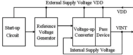
Fig. 1 The architecture of VDC
fluctuations, say 10%, without excessive additional circuitry. Without circuitry having some slight voltage increase along the ambient temperature, memories typically experience slower access. It is also to allow some tolerance on internal voltage affected by parameter variations during a silicon fabrication process[1][2]. These are the reasons, in semiconductor memory devices, to achieve both low power operation and stability in operation, of which an on-chip DC-to-DC Voltage down converter (VDC) is strongly desired.
In this paper, we propose a voltage-up circuit basedVDC. Employing a bandgap reference(BGR) based on vertical parasitic bipolar in n-well, the circuit achieves good insensitivity characteristics of
temperature and external supply voltage. Therefore, it is suitable for the low-power memory chips.
II. Analysis of Conventional VDC A voltage down converter for converting an external power voltage into an internal power voltage and providing the internal power voltage to an internal circuitry comprising is defined by: a reference voltage generation means for receiving the external power voltage and generating a constant reference voltage where variation of the external power voltage and change of circumstance temperature are compensated; a reference voltage converting means for converting the reference voltage from the reference voltage generation means into a reference voltage for stress mode or a reference voltage for normal mode; and a driving means for receiving the references to generate the internal power voltage required to operation of the internal circuitry.
The architecture of the conventional VDC is shown in Fig.1. The basic blocks include a start-up, a reference voltage generator, a voltage-up converter, and a pass device circuit with low output impedance and large driving capability[3][4].
2.1 Reference voltage generator
A reference voltage generator(RVG) with low sensitivity to temperature and supply voltage is commonly required in analog or digital circuits. To begin with, there are three types of reference voltage generator using MOS transistors only:
threshold-based generators, threshold difference based generators and thermal voltage based generators[5][6]. Unlike the bipolar type generators, these reference generation circuits are compatible to the standard CMOS process, whereas BJT type's reference generators provide with an excellent temperature coefficient. It has temperature dependency of less than 1mV/℃ and supply voltage dependency of 2mV/V, which are pretty good values. But, it has some drawbacks of an additional diffusion step in silicon fabrication making process complex and inferior device reliability and model in accuracy. To overcome the difficulties related to the parasitic transistors of MOS structure, BiCMOS type devices are being employed since it provides
with a handy design parameters. It should be noted that an ideal BJT is not available in CMOS
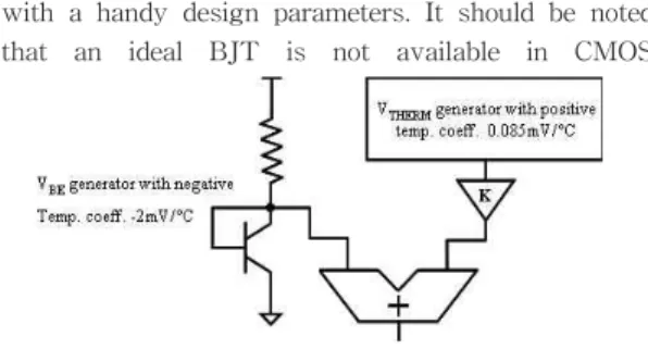
Fig. 2 Structure of a bandgap RVG
technology. A pnp BJT is made using the n-well normally associated with a pMOS[7] behaving the p-substrate as the collector.
Designs of band-gap reference voltage generators report the temperature dependency issue complying with the coefficient limit less than 100ppm/℃. Two circuits, each having opposite polarity in temperature coefficients, are merged so that the temperature dependencies cancel out each other. The structure of a bandgap reference voltage generator is shown in Fig.2, which consists of a VBE generator and a VTHERM generator. The VBE generator has the temperature coefficient of -2mV/℃ and the VTHERM
generator has the coefficient of +0.85mV/℃. The output of the VTHERM generator is amplified to match the temperature coefficient of the VBE
generator, which are merged to yield the reference voltage[8].
2.1.1 Temperature dependency of Vref
There are several methods to realize a temperature independent voltage. The base emitter junction used as a core component of the bandgap reference is the most popular approach. The general bandgap reference voltage is described by a linear combination of base-emitter voltage. We can compensate temperature dependent voltage by adding a positive-TC(temperature coefficient)voltage to a negative-TC voltage[9]. The temperature behavior of a pn-junction voltage is described by
ln
, (1) where VT is the thermal voltage. With T at room temperature and VBE=750mV,
≈
The positive-TC voltage comes from the voltage difference between two pn-junction.
∆ ln
ln
ln
(2)
where n equals to the current density ratio of Q2 to Q1. Ideally, adding a positive-TC voltage to a negative-TC voltage can realize a zero TC 1.25V at the room temperature. Additionally, the reference voltage is required to be robust to the power supply voltage. An easy way to improve power supply rejection ratio(PSRR) is to increase the open loop gain.
2.1.2 Range of the external supply voltage
A conventional CMOS bandgap reference circuit is shown in Fig.3[10]. Here the output bandgap reference voltage is given by
ln
(3)
where A1 and A2 are the emitter areas of Q1 and Q2. The first term to right in equation (3) is a complimentary to absolute temperature(CTAT) voltage and the second term a proportional to absolute temperature(PTAT) voltage. temperature independent voltage is obtained by adding these two voltages. The minimum supply voltage(VDD(MIN)) required for the operation of this circuit is given by
(4)
for conventional BGR Vref=1.25V. VSDsat3 can vary from 0.1 to 0.3V depending on the process, resulting in a VDD(MIN) of around 1.4V. Further the limitation on VDD(MIN) comes from the operation amplifier; we need to ensure that the operational amplifier can also work at this supply voltage. A technique to achieve sub 1V bandgap reference voltage is discussed in [11], but the operational amplifier in that design requires a VDD(MIN) of 1.5V. So design of low voltage bandgap reference circuits are limited by the supply voltage requirements if the operational amplifier is designed to work with a minimum supply voltage of 900mV.
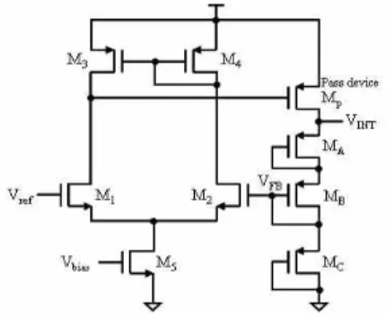
2.2 Voltage-up converter
Fig. 4. shows the conventional voltage-up circuit including a differential amplifier, a pass device, and a level shifter[3]. The level shifter adopts long channel pMOS transistors including MA∼MC and the two transistors MA∼MB are entirely the same.
Since these devices are in a saturation region, the
current can be expressed as
(5)
Fig. 3 CMOS bandgap reference circuit
Fig. 4 Voltage-up circuit
where is the transistor gain factor of MA and MB, is that of MC, and is the threshold voltage of the transistors. and are initially identical and are changed by blowing the fuses. If the gain of the amplifier is sufficiently large, the feedback voltage VFB is nearly equal to Vref.
III. Design and Analysis of Proposed VDC
This paper relates to a circuit for generating a reference voltage in a semiconductor device and particularly to an internal voltage down converter which produces an internal supply voltage by down-converting an external supply voltage.
3.1 Design of proposed VDC
Two aspects are important in voltage down
converter design: lower impedance of power supply node and stabilization of the DC output level. It is difficult to an optimized design for both design concerns at the same time. Two different approaches are employed to meet these design variables: internal voltage source and reference voltage source. An internal voltage source is designed primarily aiming at lower output impedance so that it can supply constant current on loads with varying impedance. A design of a voltage reference source, on the otherhand, concentrates to overcome variations in external operational conditions such as external supply voltage fluctuations and temperature changes. A successful voltage down converter is to take advantages of these two different design approaches.
3.2 Analysis of proposed VDC
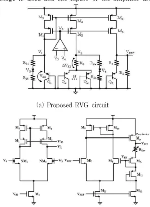
Fig. 5 is the circuit of proposed VDC, which is composed of a reference voltage generator based on bandgap reference, and a voltage-up circuit with low output impedance and high-driving capability.
The function of the RVG is to produce a stable reference voltage Vref that is free from fluctuations of external supply voltage VDD and temperature.
The proposed bandgap RVG circuit consists of a CMOS wide-swing differential-amplifier, parasitic BJTs, and resistors. The voltage-up circuit consists of a differential amplifier, a MP pass device and a level-shifter consists of a MA pMOS device, a RDrv
driving resistor and two MOSFETs M11 and M12 for voltage feedback. The wide-swing differential amplifier adjusts the internal supply voltage Vint
level to match the Vint shift level with the Vreflevel.
Because of the high drivability requirement of VDC, the pass device size of MP is relatively large.
3.2.1 Proposed bandgap RVG
Major concerns of bandgap reference circuit designs are to obtain a stable voltage level even with power supply fluctuation, process parameter scattering and ambient temperature variation.
Various circuit innovations are applied to keep an accurate and precise voltage level at the output of a reference voltage generator. We now review some of representative designs in terms of stability and immunity against power and junction temperature changes.
In this design some modifications are made to the circuit of conventional RVGs[3][6][8][11]. The main differences are that an amplifier with a nMOS input stage is used and the inputs of the amplifier are
(a) Proposed RVG circuit
(b) Wide-swing differential amplifier (c) Voltage-up circuit
Fig. 5 Proposed VDC circuit
connected to native nMOS stage instead of pMOS input stage. The resulted circuit is shown in Fig.
5(b). In addition, the output impedance of the current sources is improved by adding cascode devices. This is important in order to reduce the supply voltage sensitivity of the voltage Vref. When the sum of the voltages across R1a and R1b is equal to VEB1, the voltage with respect to ground at V3
and V4 is ⋅.
min m ax⦗×
⦘
(6)
In the original design the operational-amplifier(op- amp) inputs are connected to the voltages V1 and V2 that are roughly in 0.4V-to-0.6V level, which is
not a suitable input for an op-amp in a 1V-to-2.5V design. To overcome that the resistors R1 and R2
are divided into two series connected parts. Now the voltages V3 and V4, which are nominally set between 150 and 200mV, are in proper range for an op-amp with pMOS input transistors.
Fig. 5 (b) illustrates the structure of the native nMOS, which is easily fabricated by CMOS option process. The transistors, with V3 and V4 applied to the gates, are native nMOS transistors(VTH=-0.15V) because the threshold voltages of the enhancement- mode nMOS transistors exceed V-feedback in the standard 0.25㎛ CMOS process.
A current which is proportional to the absolute temperature(PTAT) is generated and added into a base-emitter voltage of Q3. From Fig. 5(a), M1~M6
form cascode current mirrors which can operate for lower supply voltage. The amplifier enforces V3 and V4 to have equal potential. As a result, V1 and V2
also have the same potential when R1a=R2a and R1b=R2b. Therefore, generated current is given by
⋅ln
(7) where N is the emitter area ratio, VT is the thermal voltage, and . The current I is injected to R4 by the current mirror formed by M3, M4, and M5, and this gives the reference voltage as follows:
⋅
⋅
ln
(8)A scaled-down bandgap reference voltage can be obtained by an appropriate resistor ratio of R4to R2. Moreover, trimming on the resistor ratio(ratio of R2
to R3) to achieve a good TC can be done on R1a
and R2a simultaneously. This structure is suitable for any CMOS technology to implement low-voltage bandgap reference.
3.2.2 Proposed voltage-up converter
The proposed voltage-up circuit is shown in Fig.5 (c). The voltage-up circuit can be converted the output voltage of bandgap reference Vref into a higher internal supply voltage VINT. And it should have enough current supply capability and low output impedance so that the VINT is not very much affected by the large loading current fluctuation. So the size of pass device MP is relatively large.
The circuit is composed of a feedback amplifier and
a MP, RDrv, MA, M12, and M13, which plays an important role in obtaining further accuracy in the output voltage of the voltage-up circuit. The output voltage VINT is IPTAT⋅RDrv+VTPA+VTP12+VSAT13
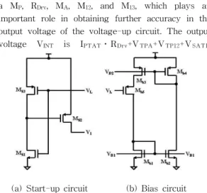
(a) Start-up circuit (b) Bias circuit Fig. 6 Design of start-up and bias for the proposed VDC
where VTPA is the built-in voltage of the threshold voltage of pMOS device. To minimize the voltage error of VINT from the nominal value VDD for a maximum Vref-range, the trimming characteristics should be designed such that any two adjacent lines pass through points(Vref, VDD-∆VINT) and (Vref, VDD+∆VINT), as suggested by the vertical broken lines in Fig.5(c).
·
(9)
3.2.3 Start-up and bias circuitry
The start-up circuit of the proposed reference circuit is shown in Fig.6(a). The RVG circuit does not operate properly if VB2 and VL follow the VDD
voltage because the bias current would become zero.
That is the reason a start-up circuit is needed for the proposed RVG. The RVG circuit has two stable operation points: one desired operating point and the other one whose current is zero when V1 and V2
are equal in Fig.5(a). To ensure that the circuit always ends up in the correct operation point a startup circuit is included. In the desired operation point the voltage V1 is above the threshold and thus the startup circuit has no effect on the RVG circuit.
The bias circuit of the proposed reference and
voltage-up circuit is shown in Fig.6(b). The op-amp and voltage-up circuit are biased by voltage bias of the bias circuit, the start-up circuit also ensures its bias current.
IV. Simulation Results
The proposed on-chip VDC is designed to provide a constant DC voltage around 1.0V with external supply voltage of 2.5V. Also, the proposed RVG can be successfully lowered in the HSPICE simulation when the threshold voltages are optimized for a low-voltage and a wide-range voltage operation.
The proposed VDC is designed with a 0.25㎛
CMOS technology.
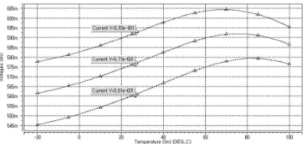
4.1 Simulation results of Vref
For the temperature effects, the simulation results are shown in Fig.7. Here, in the conventional RVG, Vref is about 1.25V, and the VDD minimum is 3.3V.
However, in the proposed RVG, the operation voltage is simply limited by the resistance ratio of R1, R2, and R4 and little influenced by the absolute value of the resistance. So the VDD minimum varies with the temperature. Fig. 7 shows the measured Vref characteristics of the proposed RVG. Vref is 0.575V( at 27℃)±0.015V from -20℃ to 100℃ at 2.5V supply voltage.
The proposed VDC using the designed bandgap reference voltage generator depends on the matching of current mirror. However when the supply voltage is changed, current matching of a simple current mirror will be degraded. Wide-swing cascode current mirror can be used to improve the performance. Another effective method is to make use of amplifier.
The amplifier enforces the two inputs having equal voltage and PTAT current can be obtained. The operational principle is the same as the one using current mirror. However, the supply dependence is greatly reduced since the amplifier is able to enforce the two inputs to be equal at different supply voltages. Fig. 8 shows the measured Vref
characteristics of the proposed RVG at VDD(at 2.375V, 2.5V, and 2.625V) variations.
4.2 Simulation results of VINT
The Voltage-up circuits should have enough
current supply capability and a low output impedance so that the output voltage is not very much affected by the large loading current fluctuation. Fig. 9 shows the simulated gain and
Fig. 7 Hspice result of voltage as a function of temperature
Fig. 8 Hspice result of voltage as a function of temperature at variations
Fig. 9 Frequency response of the voltage-up converter
phase versus frequency for voltage-up with p-type pass transistor MP. When the load impedance
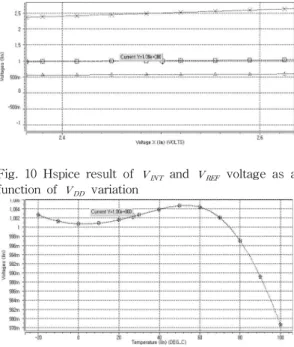
varies from 10Ω to 2㏀(Rload from 100mA to 0.5mA), the phase margin is only among 60° to 90°, enough to ensure the loop stability for semi- conductor device. Fig.10 is the simulation result of VINT for different supply voltages, which can provide a stable voltage around 1.0V with external supply voltage of 2.5V. A capacitance Cload=20PF and resistance Rload=3㏀ are used as the load impedance. Only ±0.12% deterioration of VINT for
±5% variation of supply voltage VDD is achieved.
For temperature effects, the simulation results shown in Fig.11 indicate that the temperature dependency of VINT is only 0.2mV/℃ with the temperature ranging from -20 to 100℃. The simulation results shown in Fig.12 indicate that the proposed VDC can provide a maximum output current of 100mA when the output voltage VINT is stabilized about 1.0V. Fig.12 shows the simulated result of VINT for different load current. VINT is among 1.0022V to 1.0044V when the load current changes from 0 to 100mA. Fig.13 shows the simulated transient response of the VDC. The output of the VDC can stabilize very quickly when the output impedance is varying. The transient response time is only 0.6㎲. Besides the pMOS pass device(Mp), the total current of VDC 13.2㎂, which requires standby power dissipation of 33.0㎼.
The output voltage() is stabilized around 1.0V.
Because the negative feedback in the voltage-up circuit can offer an adequate phase margin, and the output of the VDC will stabilize very quickly when the output impedance is varying. If a shorter transient response time is required, the voltage-up circuit should be biased at a higher current, which will take a larger power dissipation on standby mode of the VDC. Finally, the performance comparison of existing VDC is summarized in Table. 1.
Fig. 10 Hspice result of and voltage as a function of variation
Fig. 11 Hspice result of voltage as a function of temperature
Fig. 12 Hspice result of as a function of output current
Fig. 13 The transient characteristic of the
Key features list [3] [4] Proposed 5.0╶3.3[V] 3.3╶1.8[V] 2.5╶1.0[V]
Supply voltagvariation
vs. Output voltage[V] 3.295~3.305 1.774~1.801 0.985~1.015 Temperature variation
vs. Output voltage[V] 3.265~3.355
(-40~100℃) 1.778~1.801
(0~70℃) 0.979~1.005 (-20~100℃) Load current variation
vs. Output voltage[V] 3.266~3.3
(0~100mA) 1.793~1.801
(0~100mA) 1.002~1.004 (0~100mA)
Transient response[㎲] 0.6 0.6
Standby power[㎼] 98.32 37.32 33.0 Table 1. Performance comparison of proposed VDC
V. Conclusion
An on-chip VDC for analog and digital mixed circuit has been developed. It uses a negative-type voltage-up circuit with stability, relatively small temperature dependency, and small standby power dissipation. Therefore, it is well suited for low power IC chip. It converts 2.5V supply voltage to 1.0V in the internal supply voltage. In HSPICE simulation results, internal voltage is bounded (about 1.0V) in the proposed circuit when transient rapidly increases during 0.6㎲. It has a couple of good characteristics such as low temperature dependency of only 0.2mV/℃ and small voltage deviation within
±0.12% for ±5% variation of power supply voltage. This circuit is designed with a 0.25㎛
CMOS technology.
References
[1] Hideto Hidaka, Kazutami Arimoto, "A 34-ns 16-Mb DRAM with Controllable Voltage Down Converter", IEEE Journal of Solid-State Circuit, Vol.
27, No. 7, pp.1020-1027, July 1992.
[2] Shyh-Jye Jou and Tsu-Lin Chen "On-Chip Voltage Down Converter for Low-Power Digital System", IEEE Transactions on Circuits and Systems, Analog and Digital Signal Processing, Vol. 45, No. 5, pp. 617-625, May 1998.
[3] Qianneng Zhou, Mingyan Yu, Jianguo Ma, and Yizheng Ye, "On-chip DC-DC voltage down converter for low-power IC chip" ASICON 2005.
6th International Conference, Vol. 1, pp.646-650, Oct.
2005.
[4] Qianneng Zhou, Fengchang Lai, and Yongsheng Wang, "On-Chip Voltage Down Converter Based on Moderate Inversion for Low- Power VLSI Chips" VLSID 2007. 20th International Conference, pp433-438, Jan. 2007.
[5] Nicollini, Germano and Senderowicz, Daniel, “A CMOS Bandgap Reference for Differential Signal Processing”, IEEE JSSC, vol.26, pp.41, January 1991.
[6] Andrea Boni, " Op-Amps and Startup Circuit for CMOS Bandgap References with Near 1-V Supply,"
IEEE Journal of Solid-State Circuit, Vol.37, No. 10, pp.1339-1343, October 2002.
[7] G.Ripamonti, M.Bertolaccini, R.Peritore, and S.Schippers, "Low Power-Low Voltage Band Gap References for Flash-EEPROM Integrated Circuits:
Design Alternatives and Experiments" Proc. of ICECS '99, Vol. 2, No. 5-8, pp.635-638, Sept. 1999.
[8] Ka Nang Leung, Philip K. T. Mok, and Chi Yat Leung, "A 2-V 23-uA 5.3-ppm/℃ 4th-Order Curvature-Compensated CMOS Bandgap Reference,
"IEEE Proc. 2002 Custom Integrated Circuits Conference, No. 12-15, pp 457-460, May 2002.
[9] Behzad Razavi, Design of Analog CMOS Integrated Circuit, McGRAW-HILL, 2001.
[10] Jing, Yueming, and Lee, Edward, "Design of Low-Voltage Bandgap Reference using Trans- impedance Amplifier", IEEE Trans. TCASII, Vol. 47, pp.552-555, June 2000.
[11] Ka Nang Leung and Philip K.T. Mok," A Sub-1-V 15-ppm/℃ CMOS Bandgap Voltage Reference Without Requiring Low Threshold Voltage Device," IEEE Journal of Solid-State Circuits, Vol.
37, No.4, pp.526-530, April 2002.
[12] Koichiro Ishibashi, "A Voltage Down Converter with Submicroampere Standby Current for Low- Power Static RAM's.", IEEE IEEE Journal of Solid-State Circuits, Vol.27, No. 6. June 1992.
BIOGRAPHY Seo Hae-jun (Member)
2001: BS degree in Electronics Engineering, Cheongju University.
2004: MS degree in Electronics Engineering, Chungbuk University.
~Present:
Ph.D course in Electronics Engineering, Chungbuk University.
Kim Young-woon (Member)
2007: BS degree in Electronics Engineering, Chungbuk
University.
~Present:
Master course in Electronics Engineering, Chungbuk University.
Cho Tae-won (Member)
1973: BS degree in Electronics Engineering, Seoul University.
1986: MS degree in Electrical Engineering, Louisville University.
1992: Ph.D degree in Electrical Engineering, Kentucky University.
~Present: Professor in School of Electrical and Computer Engineering, Chungbuk University.