Printed in the Republic of Korea https://doi.org/10.5012/jkcs.2019.63.2.94
Synthesis and Characterization of Nb, Mo-doped and Nb/Mo-codoped Monoclinic VO
2Nanoparticles and Their Thin Films by Hydrothermal/Post-Thermal
Transformation and Wet-Coating Method
Jongmin Kim, Young Hee Jung†, Jun Young Kwak†, and Yeong Il Kim*
Department of Chemistry, Pukyong National University, Pusan 48513, Korea.
†Research Laboratory, Adchro, Inc. Busan 48547, Korea. *E-mail: [email protected] (Received January 14, 2019; Accepted January 31, 2019)
ABSTRACT. Nb, Mo-doped and Nb/Mo-codoped VO2(M) nanocrystallites with various doping levels were synthesized for the first time by a hydrothermal and post thermal transformation method. The reversible phase transition characteristics of those doped VO2(M) was comparatively investigated. Nb-doping of VO2(M) by this method resulted in a very efficient lowering of the transition temperature (Tc) with a rate of -16.7oC/at.% that is comparable to W-doping, while Mo-doping did not give a serious reduction of Tc with only a rate of -5.1oC/at.%. Nb/Mo-codoping gave a similar result to Nb-doping without a notice- able difference. The thin films of Nb-doped and Nb/Mo-codoped VO2(M) with a thickness of ca. 120 nm were prepared by a wet-coat- ing of the nanoparticle-dispersed solutions. Those films showed a good thermochromic modulation of near infrared radiation with 30-35% for Nb-doped VO2(M) and 37-40% for Nb/Mo-codoped ones. Nb/Mo-codoped VO2(M) film showed slightly enhanced thermochromic performance compared with Nb-doped VO2(M) film.
Key words: VO2(M), Thermochromic, Semiconductor-to-metal phase transition, Nb-doping, Nb/Mo-codoping
INTRODUCTION
Monoclinic VO2(M) has attracted extensive interests on its phase transition behavior since Morin showed the abrupt conductivity change from metallic to nonmetallic behavior with decreasing temperature in some metal oxides including VO2(M).1 The electrical transition from semiconductor to metal of VO2(M) is accompanied by the crystal phase tran- sition from monoclinic to tetragonal rutile structure.2 This transition enables its optical property in infrared region to be changed depending on temperature and makes it useful for smart window applications as a thermochromic material.3 However, its transition temperature (Tc), that is about 68oC, is too high to be practical for a real life. Doping of VO2(M) with higher valent cations such as W6+, Mo6+, Nb5+ and Ta5+
than V4+ was known to lower Tc.4 The reduction of Tc by these cations were usually explained by the extra electrons introduced by the higher valent cations5 and the compres- sive strain introduced by larger ion size.6 But it is not clearly revealed so far. Among these cations W6+ was known to be the most effective dopant with a rate of -20 ~ -28oC per atomic (at.) % vs V.4, W6+-doping could reduce Tc easily to a practical temperature but the transition sharpness also quickly decreased as the doping level increased and its thermo- chromic performance was reduced. Although there were so many studies of W-doped VO2(M),7 doping of Nb and
Mo into VO2(M) has not been well investigated because the reduction of Tc was known to be much less effective than W-doping. The early studies showed that both Nb- and Mo-dopings decreased Tc at a rate of about -7~-10oC/
at.% that was less than a half of W-doped one.8
For the practical purpose to apply this thermochromic material to smart window, the preparation of its thin film is important as well as its transition property. Although there are some methods of fabricating VO2(M) thin film such as chem- ical vapor deposition (CVD), magnetron sputtering and sol- gel methods, the most cost-effective method of preparing thin films on any kind of substrate is wet-coating method without high-temperature thermal treatment using coating solution including well-dispersed functional materials. It is essential to prepare functional nanoparticles as smaller as possible for this coating method. Most of previously reported Nb or Mo doped VO2(M) films had been prepared by CVD9, magnetron sputtering10, and pulsed laser meth- ods.11
In this study we report for the first time the preparation of Nb, Mo or Nb/Mo codoped VO2(M) nanoparticles by the thermal transformation of the doped VO2(B) that was first prepared by hydrothermal reaction and their thin films that were prepared by wet-coating method using these nanopar- ticles-dispersed solutions. Their phase transition characteris- tics were comparatively investigated.
EXPERIMENTAL
Materials and Preparation
Vanadium (V) oxide (V2O5, 99.2%), niobium (V) oxalate hydrate (Nb(HC2O4)5·xH2O), ammonium molybdate (para) tetrahydrate ((NH4)6Mo7O24·4H2O, 99%) were purchased from Alfa Aesar. Anhydrous oxalic acid (H2C2O4, 95%) were obtained from Kanto Chemical. The hydration num- ber of niobium (V) oxalate was determined as 2.4 by thermal gravimetric analysis. Polyethylene terephthalate (PET) film with thickness of 40 μm and 0.7 % haze was purchased from Toray Chemical. All chemicals were used without fur- ther purification. Water was purified to 18.1 MΩ with Barn- stead Nanopure water purification system. The syntheses of undoped and doped VO2(B) and VO2(M) were done by following the procedure previously described in detail.12 Briefly, for the synthesis of VO2(B), H2C2O4 and V2O5 with 2: 1 molar ratio were first reacted in water at about 60 oC for 24 h. The reacted solution mixture was transferred to an autoclave and kept at 200oC for 24 hr. For doping, the appropriate amounts of niobium oxalate and ammonium molybdate were directly added to the reaction mixture and stirred for 2 h just before hydrothermal reaction. VO2(B), whether it was doped or not, was transformed to VO2(M) by being heated under argon gas flow at 600oC for 2 h. VO2(M) thin film on PET substrate was prepared by bar-coating with VO2(M)-dispersed coating solution. The coating solutions were prepared by ball-milling the suspension of the sample powders in the mixed solution of ethanol and water (4:1 v/v) with zirconia bead for 5 days.
Characterization
The X-ray diffraction (XRD) patterns were obtained from Phillips X'Pert-MPD diffractometer using Cu Kα radiation source at a scan rate of 0.02o s-1 in the 2θ range of 5-80o. The instrumental line broadening of XRD was calibrated using Si 630c standard reference material by controlling slit width. Field-emission scanning electron microscopic (FE-SEM) and transmission electron microscopic images (FE-TEM) were taken with Jeol JEM-6700F, Jeol JEM- 2100F electron microscopes, respectively. Differential scan- ning calorimetry (DSC) and thermogravimetric analysis (TGA) were carried out by Perkin-Elmer Pyris 1 with a heat- ing rate of 5 oC/min in nitrogen atmosphere. Temperature- dependent visible and near-infrared (NIR) spectra were measured by using JASCO V-670 UV-VIS-NIR spectro- photometer equipped with a Peltier thermostatted sample holder. Bar-coating for thin film was performed with BMS Tech VT-300D auto film applicator. The amounts of Nb and
Mo in doped VO2(M) were analyzed with X-ray fluorescence spectrometer (Shimadzu XRF-1700). The film thickness was measured with Tencor AlphaStep 500 profilometer.
RESULTS AND DISCUSSION
The doped and codoped VO2(M)s with Nb and Mo were prepared by the thermal transformation of doped VO2(B) that was synthesized by hydrothermal reaction as previ- ously described by us.12 Nb-doped, Mo-doped and Nb/
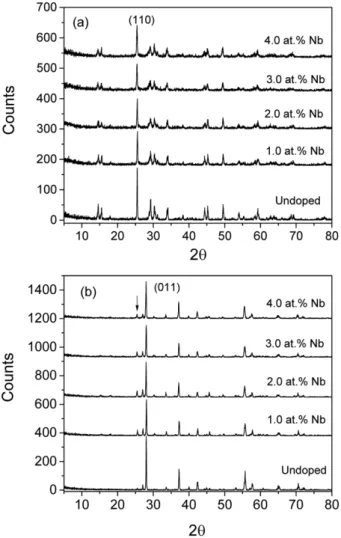
Mo-codoped VO2 will be denoted as Nb-VO2, Mo-VO2 and Nb/Mo-VO2 hereinafter. Fig. 1 and 2 show XRD patterns of Nb- and Mo-VO2, respectively with 0-4.0 at.% fed amounts of Nb and Mo dopants. Regardless of the fed amounts of dopants, all XRD patterns show the well-characterized peaks of VO2(B)13(a) and VO2(M).13(b) After the transformation to M phase, the small impurity level of B phase remained
Figure 1. XRD patterns of (a) B and (b) M phases of Nb-VO2
samples with various fed amounts of Nb (The arrow indicates (110) peak of B phase).
for Nb-doped VO2(M) as indicated with an arrow in Fig.
1(b) while it did not for the undoped one. This impurity B phase also appeared for W-doped VO2(M) that was pre- pared by this method.12 However, it is far less for Mo-VO2 as shown in Fig. 2(b). As the amounts of Nb dopant increase, the major peak intensities slightly decrease and the peaks become broader for both B and M phases of Nb-VO2. This means that the crystallites of both phases become systemati- cally smaller with increased doping. For the case of Mo-VO2,
however, M phase crystallite does not decrease while B phase does. Using the most intense peaks, (110) and (011) of B and M phases, respectively, the crystallite sizes are estimated by Scherrer equation14 and listed in Table 1. The actual doped level was analyzed semi-quantitatively with XRF and are also listed in Table 1. The actual doped amounts of both Nb and Mo decreased from about 80% to 60% of the fed amounts as the fed amounts increased from 1.0 at.%
to 4.0 at.% vs vanadium atom. For comparison, our previous study showed that tungsten was doped in almost 100% if the fed amount was less than 1.5 at.% in the same synthetic method.12 While the crystallite sizes of both Nb- and Mo- VO2(B) are very similarly decreased with the increased dop- ing level, those of Nb- and Mo-VO2(M) are quite different.
The crystallinity of Mo-VO2(M) is barely affected by the dopants while the size of Nb-VO2(M) slightly decreases with the increased doping level. Anyhow, the crystallite sizes of these doped VO2(M) are in the range of ca. 30-57 nm for these doping levels. On the other hand, W-VO2(M) with 1.5 at.% doping was less than 30 nm.12
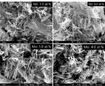
The morphologies of the doped VO2(B) and VO2(M) are shown in Fig. 3 and 4, respectively as FE-SEM images.
Figure 2. XRD patterns of (a) B and (b) M phases of Mo-VO2
samples with various fed amounts of Mo.
Table 1. The estimated crystallite sizes of B and M phases of Nb- and Mo-VO2 with various doping levels
Fed (at.%) Nb-VO2 Mo-VO2
Doped (at.%) B (nm) M (nm) Doped (at.%) B (nm) M (nm)
0.0 0.0 55.4 55.5 - - -
1.0 0.8 42.6 49.1 0.8 47.0 55.5
2.0 1.7 39.4 48.9 1.3 41.8 50.9
3.0 2.0 36.5 45.3 2.0 35.4 53.6
4.0 2.4 31.7 39.2 2.3 32.7 57.1
Figure 3. FE-SEM images of Nb- and Mo-VO2(B) with two dif- ferent fed amounts of dopants (Bar scale: 1 μm, Magnification:
×10,000).
The B phase morphologies that were prepared by hydro- thermal reaction are all similar and thin rod-like with aspect ratio of ca. 10-20 regardless of the type and amount of dopant. Both the B and M phases of VO2 that were pre- pared by direct hydrothermal reaction were reported to have usually rod-like or belt-type morphologies whether they were doped or not.15 When these VO2(B) were trans- formed to VO2(M) by thermal treatment, the morphologies were slightly changed to partly spherical shapes with fused forms each other. The fusion seemed to be more prominent for Mo-VO2(M) than Nb-VO2(M). The amounts of dopants barely affected the sizes of the fused forms.
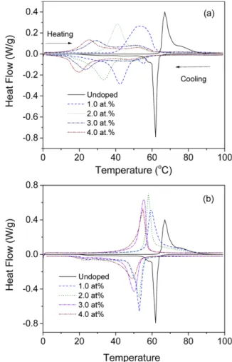
The phase transition properties of Nb-VO2(M) and Mo- VO2(M) were characterized by DSC. Fig. 5 shows DSC data demonstrating the doping effect on Tc and the hysteresis of the phase transition. The effect of two dopants on the transition characteristics is dramatically different. While Nb-VO2(M) shows large Tc shift depending on doping level, Mo-VO2(M) shows a small dependence on the dopant. And while the transition sharpness of Nb-VO2(M) decreases with increasing doping level, that of Mo-VO2(M) is not reduced at all. All Nb-VO2(M) samples show a small minor transition at
the temperature higher than the major Tc. These minor transitions may be ascribed to the inhomogeneity of the spatial distribution of the dopant. Tc and the temperature hyster- esis (ΔTc) of these doped VO2(M) are listed in Table 2. In order to depict the doping level dependence of Tc, the plots of Tc vs doping level are shown in Fig. 6. For both the dop- ants, the dependence is almost linear with quite different slopes. The reducing rates of Tc from the slopes are -16.7 and -5.1oC/at.% for Nb and Mo, respectively. According to the previous studies of thin films of Nb-doped VO2(M) Figure 4. FE-SEM images of Nb- and Mo-VO2(M) with two dif-
ferent fed amounts of dopants (Bar scale: 1μm, Magnification:
×10,000).
Figure 5. DSC curves of (a) Nb- and (b) Mo-VO2(M) with vari- ous fed amounts of dopants (The baseline was subtracted.).
Table 2. The estimated transition temperatures and hysteresis of Nb- and Mo-VO2(M) from DSC data according to doping level
Fed amounts (at.%) Nb-VO2(M) Mo-VO2(M)
Doped (at.%) Tc (oC) ΔTc (oC) Doped (at.%) Tc (oC) ΔTc (oC)
0.0 0.0 64.5 5 0.0 64.5 5
1.0 0.8 47.5 11 0.8 56.3 6.5
2.0 1.7 37.5 7 1.3 55.5 5
3.0 2.0 26.0 6 2.0 52.8 5.5
4.0 2.4 22.5 5 2.3 51.0 4
that were directly prepared by magnetron sputtering,9(c) CVD10(b) and laser deposition11 methods, the reducing rates were -7 ~ -8.5 oC/at.%. Therefore, the reducing rate of our powder Nb-VO2(M) is about twice higher than that of the thin films and comparable to that of well-known W-doped VO2(M). Recently, Yuan et al. reported that Nb-VO2(M) that was prepared by the high temperature solid state syn- thesis with VO2(M) and Nb2O5 showed the reducing rate of -13 oC/at.% that is slightly lower than ours.16 In the case of W-doping, there is no report, as far as we know, show- ing considerable difference between thin film and powder samples. However, Nb-doping seems to give a quite dif- ferent result between thin film and powder samples. The reason is not clear at this point. On the other hand, our Mo- doped sample gives a slightly different rate than those of the thin films that were reported as -3oC/at.% from CVD10(b),17 and -7 oC/at.% from sol-gel method.18 The powder sample of Mo-VO2(M) that were prepared by direct hydrothermal reaction was reported to give the reducing rate of -7.86oC/
at.%.19 Therefore, it seems that Mo-doping does not cause a serious difference between thin film and powder sample, unlike Nb-doping.
In our synthetic method of doped VO2(M), Nb-doping gives a pretty efficient lowered Tc close to W-doping and the hysteresis and the transition sharpness seems to be even
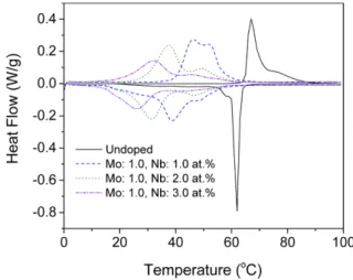
better than W-doping.20 Meanwhile, Mo-doping does not give an efficient lowering of Tc but the transition sharp- ness becomes somehow better than the undoped one as shown in Fig. 5(b). The lowering of Tc by doping always requires the sacrifice of the transition sharpness as shown with W and Nb-doping. Our previous study showed that W/Mg- codoping helped the enhancement of transition sharpness while keeping the lowered Tc.12 Therefore, we tried the codop- ing of Nb and Mo into VO2(M) with expecting a syner- gistic effect. The codoping was performed with the varied amounts of 1.0-3.0 at.% for Nb and the fixed amount of 1.0 at.% for Mo. The XRD data and the morphologies of Nb/Mo-codoped VO2 are very similar to those of Nb-doped one.21 The actual codoped levels of Nb and MO are also similar to those of separately doped Nb and Mo. The esti- mated crystallite sizes and the actual doped levels are listed in Table 3. While B phase sizes of the codoped VO2 are slightly smaller than those of Nb-doped ones, M phase sizes were slightly larger. Fig. 7 shows DSC curves of Nb/Mo-VO2(M) with various doping levels. The phase transition charac- teristics of Nb/Mo-VO2(M) depending on doping level also shows very similar tendency as that of Nb-VO2(M). The noticeable difference is that the second minor transition at higher temperature becomes slightly more recognizable at low doping level of Nb. The transition temperature and Figure 6. Doping level dependence of transition temperatures of
Nb- and Mo-VO2(M).
Table 3. The estimated crystallite sizes, transition temperatures and hysteresis of Nb/Mo-VO2(M) from XRD and DSC data accord- ing to doping levels
Fed (at.%) Doped (at.%)
B size (nm) M size (nm) Tc (oC) ΔTc (oC)
Nb Mo Nb Mo
1.0 1.0 0.8 0.7 40.7 57.6 42.5 7
2.0 1.0 1.3 0.6 36.3 49.2 34.5 7
3.0 1.0 2.3 0.6 29.5 44.0 29.0 6
Figure 7. DSC curves of Nb/Mo-VO2(M) with various fed amounts of dopants (The baseline was subtracted.).
the hysteresis are listed in Table 3. Tc of Nb/Mo-VO2(M) is slightly lower than that of Nb-VO2(M) at the same feed- ing level of Nb. However, there is no considerable enhance- ment of transition sharpness.
The thin films of Nb-doped and Nb/Mo-codoped VO2(M) was prepared on PET substrate by bar-coating method using the particle-dispersed solutions. The coating solutions were prepared by ball-milling of the sample powders in aque- ous ethanol solution. In our previous study12 we had used a block copolymer as dispersing agent and binder in organic mixed solvent. But no dispersing agent was added in this coating solution. The well-dispersed solution gave a fairly transparent and very robust film on PET substrate. In order to check the particle sizes of the samples in the coating solu- tion, TEM images of the ball-milled samples were taken and are shown in Fig. 8. The images of all samples with different doping levels are not considerably different as shown in the chosen two samples of Nb- and Nb/Mg-VO2(M).
The particle sizes are distributed in the range of 20-80 nm.
The average sizes are roughly similar to the estimated crys- tallite sizes that were about 40-50 nm. Therefore the fused par- ticles after the thermal transformation were broken down to crystallite nanoparticles by the long-term ball-milling.
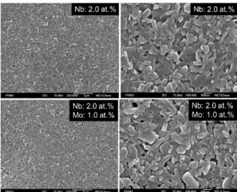
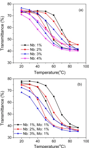
The thin films of Nb- and Nb/Mo-VO2(M) on PET also have all the similar morphologies regardless of doping levels as shown in FE-SEM images of Fig. 9. The films are all smooth without any crack and nanoporous as shown in the magnified images. The film thicknesses were con- trolled to give ca. 120 nm by the concentration of coating solution and Mayer rod number. The visible and near infra- red (N-IR) transmission spectra of these thin films were measured at the wavelengths between 350-2,500 nm and temperatures between 20-90oC. Fig. 10 shows the trans- mission spectra of Nb-VO2(M) and Nb/Mo-VO2(M) at the selected doping levels for comparison. The N-IR transmittances of all the films decrease as the temperature increases and thus
the thermochromic characteristics is clearly seen. The trans- mittance-vs-temperature curves are plotted for all the samples of Nb- and Nb/Mo-VO2(M) and shown in Fig. 11. The Figure 8. FE-TEM images of Nb- and Nb/Mo-VO2(M) after
being ball-milled in aqueous ethanol solution (Bar scale: 100 nm, Magnification: ×25,000).
Figure 9. FE-SEM images of the thin films of Nb- and Nb/Mo- VO2(M) (Bar scale:1 μm, 100 nm, Magnification: x20,000, ×80,000).
Figure 10. Temperature dependence of transmission spectra of (a) Nb-VO2(M) and (b) Nb/Mo-VO2(M) films on PET substrate. (The temperature varied from 20 to 90 oC in an increment of 10 oC).
transition temperatures and the hysteresis that were esti- mated from these optical transmittance changes are listed in Table 4. The transition temperatures for all these doped VO2(M) films that were measured from transmittance data are about 15-25oC higher and the hysteresis are wider than those of the corresponding powder samples that were measured from DSC data discussed above. This difference was also observed in our previous study for W- and W/Mg-VO2(M).12 We assumed that the difference came from the grain size difference that was caused by ball-milling.
The reduced grain size after ball-milling gave the larger
surface area and the increased surface property might have more effect, giving such a result. As the inhomogeneity of the dopant distribution was presumed from the DSC data that showed the second minor transition following the major one, the doping level of the surface may be higher than the interior and the deteriorated surface property by ball-milling may have affected on the transitions of the film samples.
Nevertheless, Nb- and Nb/Mo-VO2(M) films are com- parable to W-VO2(M) film although the doping level should be slightly higher. The N-IR transmittance changes at 2,000 nm by the phase transition, which are estimated from the difference between 20 and 90 oC data, are 30-35 % and 37- 40% for Nb-VO2(M) and Nb/Mo-VO2(M), respectively.
These values are lower than that of the undoped VO2(M) film but higher than that of W-VO2(M) with the doping level of 1.5 at.%, which were reported by 47 and 29%, respec- tively in our previous study.12 Therefore, Nb-VO2(M) film that was prepared by our method is advantageous to W- VO2(M) film in terms of thermochromic effect, even though Tc is slightly higher at the same doping level. The codop- ing of a small amount of Mo with Nb into VO2(M) definitely helps the lowering of Tc and the increasing of the optical switching efficiency as shown in Table 4.
CONCLUSION
Nb-, Mo-doped and Nb/Mo-codoped VO2(M) nano- crystallites were, for the first time, synthesized by a hydrother- mal and post thermal transformation method. Nb-VO2(M) showed the lowered Tc with a reducing rate of -16.7oC/
at.% that is comparable to W-VO2(M), while Mo-VO2(M) did not show the serious reduction of Tc with only the rate of -5.1oC/at.%. However, the doping of Mo did not cause the deterioration of transition sharpness that was observed in W- and Nb-doping. The transition property of Nb/Mo- VO2(M) is very similar to Nb-VO2(M) with a slightly lower Tc at the same doping level of Nb. The thin films of Nb- and Nb/Mo-VO2(M) that were prepared by a bar-coating of the particle-dispersed solutions shows a relatively good Figure 11. Temperature dependence of the transmittance at
2,000 nm for (a) Nb-VO2(M) and (b) Nb/Mo-VO2(M) films on PET substrate.
Table 4. Optical transition properties of Nb- and Nb/Mo-VO2(M) films on PET substrate.
Fed Nb* (at.%) Nb-VO2(M) Nb/Mo-VO2(M)
Tc ΔTc ΔT** Tc ΔTc ΔT**
1.0 62 15 32 55 10 40
2.0 57 15 30 48 12 39
3.0 55 10 35 45 10 37
4.0 45 10 34
*The actual doped levels of Nb and Mo are listed in Table 2 and 3.
**ΔT denotes the transmittance difference between the values at 20 and 90 oC measured at 2,000 nm.
thermochromic modulation of N-IR with 30-35% and 37- 40%, respectively, although Tc became higher than those of the corresponding powder samples. Nb/Mo-VO2(M) film shows that the codoping have a synergistic effect on both the lowering of Tc and the N-IR modulation efficiency.
Acknowledgments. This work was supported by the research fund of Pukyong National University (Year 2017-2018).
REFERENCES 1. Morin, F. J. Phys. Rev. Lett. 1959, 3, 34.
2. (a) Anderson, G. Acta Chem. Scand. 1954, 8, 1599. (b) Westman, S. Acta Chem. Scand. 1961, 15, 217.
3. (a) Kamalisarvestani, M; Saidur, R.; Mekhilef, S.; Javadi, F. S. Ren. Sust. Ener. Rev. 2013, 26, 353. (b) Gao, Y.;
Luo, H.; Zhang, Z.; Kang, L.; Chen, Z.; Du, J.; Kanehira, M.; Cao, C. Nano Ener. 2012, 1, 221. (c) Granqvist, C. G.;
Lansaker, P. C.; Mlyuka, N. R.; Niklasson, G. A.; Avendano, E. Sol. Energy Mater. Sol. Cells 2009, 93, 2032.
4. Goodenough, J. B. J. Solid State Chem. 1971, 3, 490.
5. (a) Tang, C.; Georgopoulos, P.; Fine, M. E.; Cohen, J. B.
Phys. Rev. B 1985, 31, 1000. (b) Zhang, J.; He, H.; Xie, Y.; Pan, B. J. Chem. Phys. 2013, 138, 114705.
6. (a) Cao, J.; Ertekin, E.; Srinivasan, V.; Fan, W.; Huang, S.; Zheng, H.; Yim, J. W. L.; Khanal, D. R.; Ogletree, D.
F.; Grossmanan, J. C.; Wu, J. Nat. Nanotechnol. 2009, 4, 732. (b) Zhang, J.; He, H.; Xie, Y.; Pan, B. Phys. Chem.
Chem. Phys. 2013, 15, 4687.
7. (a) Horlin, T.; Nikelwski, T.; Nygren, M. Mat. Res. Bull.
1972, 7, 1515. (b) Tang, C; Georgopoulos, P.; Fine, M. E.
Cohen, J. B. Phys. Rev. B 1985, 15, 31. (c) Sobhan, M.
A.; Kivaisi, R. T.; Stjerna, B.; Granqvist, C. G. Sol. Energy Mater. Sol. Cells 1996, 44, 451. (d) Li, G.; Chao, K.; Peng, H.; Chen, K.; Zhang, Z. Inorg. Chem. 2007, 46, 5787.
8. (a) Savborg, O.; Nygren, M. Phys. Status Solidi A 1977, 43, 645. (b) Kleinschmidt, P. Phys. Lett. 1974, 47A, 205.
(c) Febritchnyi, P. B.; Bayard, M.; Pouchard, M.; Hagen- muller, P. Solid State Commun. 1974, 14, 603.
9. (a) Greenberg, C. B. Thin Solid Films 1983, 110, 73. (b) Piccirillo, C.; Binions, R.; Parkin, I. P. Eur. J. Inorg. Chem.
2007, 4050. (c) Manning, T. D.; Parkin, I. P.; Blackman, C.; Qureshi, U. J. Mater. Chem. 2005, 15, 4560.
10. (a) Batista, C.; Carneiro, J.; Ribeiro, R.; Teixeira, V. J.
Nanosci. Nanotech. 2011, 11, 9042. (b) Batista, C.; Ribeiro, R.; Teixeira, V. Nanoscale Res. Lett. 2011, 6, 301.
11. Nishikawa, M.; Nakajima, T.; Kumagai, T.; Okutani, T.;
Tsuchiya, T. J. Cerm. Soc. Japan 2011, 119, 577.
12. Park, H.; Kim, J.; Jung, Y. H.; Kim, Y. I. J. Korean Chem.
Soc. 2017, 61, 57.
13. (a) JCPDS 81-2392. (b) JCPDS 43-1051.
14. Patterson, A. Phys. Rev. 1939, 56, 978.
15. (a) Liu, X.; Xie, G.; Huang, C.; Xu, Q.; Zhang, Y.; Luo, Y. Mater. Lett. 2008, 62, 1878. (b) Liu, J.; Li, Q.; Wang, T.; Yu, D.; Li, Y. Angew. Chem. Int. Ed. 2004, 43, 5048.
(c)Zhang, Y.; Zhang, J.; Zhang, X.; Deng, Y.; Zhong, Y.;
Huang, C.; Liu, X.; Mo, S. Ceram. Int. 2013, 39, 8363.
16. Zhang, R.; Yin, C.; Fu, Q.; Li, C.; Qian, G.; Chen, X.; Lu, C.; Yuan, S.; Zhao, X.; Tao, H. Cerm. Int. 2018, 44, 2809.
17. Bastista, C; Teixeira, V.; Ribeiro, R. M. J. Nanosci. Nan- otechnol. 2010, 10, 1393.
18. Hanlon, T. J.; Coath, J. A. Richardson, M. A. Thin Solid Films 2003, 436, 269.
19. Li, D.; Li, M.; Pan, J.; Luo, Y.; Wu, H.; Zhang, Y.; Li, G.
App. Mater. Interfaces 2014, 6, 6555.
20. W-doped VO2(M) that was prepared by the same method showed the reducing rate of 18.7oC/at.% and the hysteresis of 12oC at 1.5 at.% doping in our previous study (Ref. 12).
21. The XRD patterns and FE-SEM images of Nb/Mo-VO2 samples is not shown since they did not show the distinguish- able difference from those of Nb-VO2.