• 검색 결과가 없습니다.

Si PIN Radiation Sensor with CMOS Readout Circuit

N/A
N/A
Protected

Academic year: 2021

Share "Si PIN Radiation Sensor with CMOS Readout Circuit"

Copied!
9
0
0

로드 중.... (전체 텍스트 보기)

전체 글

(1)

http://dx.doi.org/10.5369/JSST.2014.23.2.73 pISSN 1225-5475/eISSN 2093-7563

Si PIN Radiation Sensor with CMOS Readout Circuit

Yu-mi Kwon, Hee-Sung Kang, Jung-Hee Lee, and Yong Soo Lee

+

Abstract

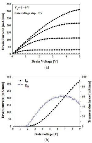
Silicon PIN diode radiation sensors and CMOS readout circuits were designed and fabricated in this study. The PIN diodes were fab- ricated using a 380-μm-thick 4-inch n+ Si (111) wafer containing a 2-kΩ·cm n- thin epitaxial layer. CMOS readout circuits employed the driving and signal processes in a radiation sensor were mixed with digital logic and analog input circuits. The primary functions of readout circuits are amplification of sensor signals and the generation of the alarm signals when radiation events occur. The radiation sensors and CMOS readout circuits were fabricated in the Institute of Semiconductor Fusion Technology (ISFT) semiconductor fab- rication facilities located in Kyungpook National University. The performance of the readout circuit combined with the Si PIN diode sensor was demonstrated.

Keywords: Si PIN diode, Si epitaxy wafer, Radiation sensor, CMOS readout circuit, Fast response

1. INTRODUCTION

The detection of excessive radiation has attracted world-wide attention since the occurrence of nuclear plant accidents such as Japan’s Fukushima nuclear crisis. Some radiation energy is very fatal and can seriously damage human organisms and/or electronic systems. Therefore, for quick detection and establishment of countermeasures against radiation incidents, a compact and portable radiation detection system used on-chip technology must be developed.

Radiation detection systems are typically used in harsh environments such as space shuttles, x-ray generators, aircrafts, weapon systems, and medical systems. Radiation sensors have been taken advantage of semiconductors as the basic materials [1-3]. Moreover, the detection efficiencies of both compound semiconductors and Si devices have been studied extensively [4-7]. Because compound semiconductors have variable bandgaps, diverse wavelength sensing applications are available [8,9]. Moreover, space charge accumulation and charge-carrier trapping that lower optical responsivity in compound

semiconductor sensors can be mitigated by using silicon [6, 10].

Therefore, in this study, we adopted a Si PIN diode for a radiation sensor connected to CMOS ROIC (readout circuit).

Different analog and digital readout circuit signals transferring diode signals to subsequent signal process steps have been developed. In this study, we employed a fast signal processing circuit and low-power consumption logic for the successful operation of the readout circuit. The CMOS ROICs were fabricated in ISFT CMOS fabrication facilities of Kyungpook National University.

2. EXPERIMENTAL

2.1 Si PIN diode fabrication

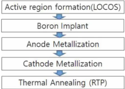
The fabrication process flow of a PIN diode is shown in Fig. 1.

PIN diodes were fabricated using a 380-um-thick 4-inch n+

Si(111) wafer having a resistivity of 0.004~0.008 Ω·cm and containing a 2-kΩ·cm n- thin epitaxial layer. Masks used for diode fabrication consist of LOCOS, ion implantation for p+ and guard- ring regions, and contact open processes for metallization.

Initially, active region isolation between devices was performed using the LOCOS process. Subsequently, boron ions were implanted in the p+ and guard-ring regions at 50 KeV with a dose of 1 ×10

15

cm

−2

. A 300-nm-thick SiO

2

film was subsequently deposited using TEOS to prevent the out-diffusion of implanted ions, and then, the samples were activated at 1000

o

C for 2 hrs in N

2

ambient. After the annealing process, the TEOS layers were School of Electronics Engineering, Kyungpook National University

80 Daehakro,Bukgu, Daegu, 702-701,Korea

+

Corresponding author: [email protected] (Received: Dec. 27, 2013, Accepted: Jan. 17 , 2014)

This is an Open Access article distributed under the terms of the Creative Commons Attribution Non-Commercial License(http://creativecommons.org/

licenses/bync/3.0) which permits unrestricted non-commercial use, distribution,

and reproduction in any medium, provided the original work is properly cited.

(2)

selectively etched in a BOE solution to open the active regions.

TiN/Al (30 nm/300 nm) anodes were deposited using a metal sputtering process followed by selective etching. In addition, for the rear cathode, Ti/Al (30 nm/300 nm) metal layers were formed with an electron-beam evaporator. Finally, an RTP process was performed to improve metal adhesion.

The device structure and photograph of the fabricated PIN diode are shown in Fig. 2. The final 2 mm diameter rounded shape

of the PIN diode was achieved several rounds of experiments. The gap between the devices namely the width of the LOCOS regions is 1 mm from edge of the 50-µm-wide guard-rings. The fabricated devices were diced with a saw blade and a laser cutting system for inspecting leakage current on the side-walls. Thereafter, the fabricated diodes were packaged in TO-cans for the long-term stabilization and measurement of radiation effects.

2.2 CMOS readout circuits design and fabrication The CMOS ROIC used for driving and signal processing in the radiation sensor was mixed with digital logic and analog input circuits. The primary functions of readout circuits include sensor signal reading and warning signal or system shut down signal generation when an excessive energy radiation excess status occurs. In addition, the signal processing circuit includes a pulse timer circuit to enable the re-operation of a system after the warning signal disappears, which is an auxiliary function of the electronic system reset. A set-reset (SR) latch that provides a flag signal was used for indicating that a radiation has been sensed.

The readout circuits have been referred to as a radiation-event detector (RED) in this paper.

The block diagram of the digital part of the RED readout circuit is shown in Fig. 3, and the functions of the circuit are listed in Table 1. The RED circuit comprises four inputs and several outputs. The four inputs are a radiation-events comparator output (RECO), a 1 MHz clock (clk1M), an external reference input signal (ref), and a radiation-event flag reset (RFR). The RECO signal is generated from an open-loop comparator with inputs of the amplified sensor signal and reference voltage. The outputs include radiation event output (RO), radiation event flag (RF), and counter signals. The operation principle of the circuit is as follows.

First, the RECO input signals from the output of the PIN diode Fig. 1. Fabrication process flow of PIN diode.

Fig. 2. (a) Structure and (b) photograph of fabricated PIN- diode. Fig. 3. Block diagram of readout circuit.

(3)

sensor enter two SR latches. If RF signal is generated, it indicates that a radiation event has occurred. If an RO signal is generated, it indicates that an excessive radiation status has occurred. Second, the RF output from the SR latch enters the AND2 gate, frequency divider (divide10), and SYNCO (13-bit synchronous counter) simultaneously. Subsequently, the AND2 gate receiving the clk1M (clock signal of 1 MHz) can be activated. As a result, the divide10 counter outputs the divided signals of 100 KHz, 200 KHz, and 500 KHz. Among these divided frequencies, the 100 KHz terminal is connected to SYNCO.

The synchronous counter can count up to 8192 steps, which is an input of the comparator. When the ref input signal matches with the SYNCO output, a signal referred to as comat will be

generated. Third, this comat signal enters the OR2 gate located in front of the SR latch generating the RO signal. As a result, the SR latch maintains the RESET and RO signals at a low level. Finally, an external RFR signal is applied for initialization, and the SR latch maintains the reset status. Further, each part of the circuit such as frequency divider, SYNCO, and comat can be monitored using the output of the operation checking procedure.

2.3 Circuit simulation

The simulation results of the CMOS readout circuits are shown in Fig. 4. When the RECO is produced, the RF and RO signals are immediately generated. The external clock signal of the timer clk1M is divided into divi2, divi5, divi10b, and divi10 for the control of the timer circuits. When the divi10 and the SYNCO [3] of the external reference “0009” signal match, the comat will be generated and RO enters the reset state. When an RFR occurs, all the signals are reset before the RECO signal reoccurs.

2.4 Mask design of RED circuit

Fig. 5 shows the mask layout of the CMOS readout circuits.

The circuit consists of 10 mask layers: n-well, LOCOS, gate, n+

implant, p+ implant, contact area open, 1

st

metal, via open, 2

nd

metal, and pad. Test patterns are prepared for analyzing of CMOS device characteristics such as resistance, capacitance, and MOSFETs. A bar-type sheet resistance measurement pattern with a length of 100 µm and width of 15 µm was designed. TLM pattern for the measurement of contact resistance was designed with a width of 200 µm and a contact area of 45 µm

2

with a separation of 30, 40, 50, 60, and 70 µm between contacts. The capacitance pattern was designed with a width of 365 µm wide.

The NMOSFET and PMOSFET of unit device were designed with a length of 2 µm and width of 40 µm.

Table 1. Description of input-output signals I/O Name of signal Characteristics Input Radiation Event

Comparator Output (RECO)

Trigger signal of NED circuit Output signal of PIN diode can be applied in RECO

Radiation Event Flag Reset (RFR)

External input signal for RF reset Clk 1M Clock signal of 1MHz for operation of

system ref

[12 … 0]

External input signal for time setup of RO reset

(Time can be controlled by 13-bit binary)

Output Radiation Event Output (RO)

Output signal of RED

RO signal can generate warning signal Radiation Event

Flag (RF)

Flag signal to indicate radiation event RF can be reset by only RFR comat When synchronous counter state and

ref signal match, “1” is generated SYNCO

[12, 9, 6, 3]

Signal for confirmation of 13-bit syn- chronous counter operation

Divi10 Signal for confirmation of frequency divider operation

Used as system clock Frequency = clk1M/10

Divi10b Signal for confirmation of frequency divider operation

Divide 10 is non-overlapping with divide 10b

Frequency = clk1M/10

Divi5 Signal for confirmation of frequency divider operation

Frequency = clk1M/5

Divi2 Signal for confirmation of frequency divider operation

Frequency = clk1M/2

Fig. 4. Simulation results of CMOS circuit.

(4)

2.5 Fabrication of CMOS circuit

The fabrication process flow of the CMOS readout circuits is shown in Fig. 6. The CMOS circuits were fabricated on 6-inch p- type (100) Si substrates with a thickness of 650 µm and a resistivity of 0.004~ 0.008 ·cm. To fabricate the CMOS circuits, n- and p-well regions were formed by injecting phosphorus and boron ions. After activation of the implanted ions followed by annealing, LOCOSs having an oxide thickness of 5200 Å were grown outside the active region for isolating each device.

Thereafter, phosphorus ions were implanted in MOSFET channels for controlling work function. Thin 250 nm gate oxides and 200 nm phosphorus-doped polysilicon gates were stacked sequentially on the MOSFET gate area for n-type formation. An inductively coupled plasma (ICP) etching process was used for gate patterning in polysilicon, and arsenic and boron ions were implanted for source and drain formation by implantation, respectively. Subsequently, a 300-nm-thick-oxide was grown using a tetraethyl orthosilicate (TEOS) process for contact open.

E-beam evaporated Ti/TiN (40 nm/800 nm) at a metal/Si contact area was used for silicide formation using rapid thermal processing (RTP) at 900

o

C for 5 min in N

2

ambient. The 1

st

metallization with Ti/Al/TiN (10 nm/300 nm/80 nm) was performed immediately after silicide formation. A 500-nm- thick oxide was deposited again on 1

st

metal surface for 2

nd

metallization. Finally, after via open, the 2

nd

metal of Ti/Al/TiN (10 nm/450 nm/80 nm) was deposited and patterned finally. After fabrication, the readout circuits were separated by sawing and packaged on a PCB using a wire bonder.

2.6 Measurement of readout circuit

A field programmable gate array (FPGA) that generates driving pulses of CMOS readout circuit was used for the characterization of readout circuit. The RFR, clk1M, and RECO having a pulse width of 80 ns pulse were applied from the FPGA to the readout circuit operated at a bias voltage of 3 V. The RECO for the verification of operation was generated 3 µs after RFR generation was used. The value of ref supplied from the timer circuit was fixed to be “1001”. The outputs of the RF and RO were generated through an inverter, which can compensate for the voltage drop.

When the circuit is connected to the PIN diode, FPGA can be replaced with RECO. The anode of the PIN diode was connected to 72 Ωk and 10 Ωk parallel resistors. The output of the PIN diode can be acquired at the resistor nodes. This output can be connected to the RECO input terminal of the circuit. Moreover, the RFR, clk1M, and ref, which were the inputs of the circuit, were applied by the FPGA.

Each component of circuit, such as the frequency divider and the synchronous counter was verified by checking the output of the comat signal.

2.7 Measurement of electrical characteristics of PIN diode

The electrical characteristics of the fabricated PIN diodes were

measured in the dark at room temperature. The top of the diode

anode in direct contacted with probe tip, and rear of the diode

cathode was connected through aluminum paste and plate. The

Fig. 5. Mask layout of CMOS IC. Fig. 6. CMOS readout circuit fabrication flow.

(5)

current-voltage (I-V) characteristics were measured with HP-4156 observable a photo-electric current in the reverse bias state. HP- 4284 was employed for the obtaining of reverse biased diode capacitance and a fully depleted voltage deducible from C-V characteristics. Because the capacitance significantly delays diodes response, the smallest possible depletion capacitance diode must be used.

2.8 Measurement of radiation response characteristics Radiation response characteristics of the fabricated diodes were investigated by using a simple circuit which consists of the diode, a bias resistance (R

D

) of 50, load resistance (R

L

) of 1 M, and a coupling capacitor (C

C

) of 10 nF, as shown in Fig. 7. The diode biased at a reverse voltage of 10 V was irradiated, and its radiation incident response was investigated.

3. RESULTS

3.1 Current-voltage characteristics

Fig. 8 shows the I-V characteristics of the fabricated PIN diode when the applied forward-bias voltage was varied from 0 to 2 V, and the reverse-bias voltage varied from 0 to -30 V. In case of forward-bias voltage, the current increased exponentially as voltage increased. The forward voltage (V

F

) of the fabricated diode was 0.6 V. Further, reverse leakage current (dark current)

low is an important for the generation of enough photon current because it can be a noise source when the radiation is incident to the PIN diode. The fabricated PIN diode exhibited an extremely low leakage current of 24 nA at a reverse bias voltage of 30 V owing to the surface passivation through the LOCOS process and the p+ guard-ring located in the outer part of the device, which can interrupt electron flow from the n+ bulk region to surface of the diced wafer.

3.2 Capacitance-voltage results

Fig. 9 shows (a) the capacitance-voltage and (b) depletion characteristic of the PIN diode. Since the depletion capacitance in the reversed-biased operation influences on the response speed largely due to resistance capacitance (RC) delay, the capacitance must be investigated to confirm the feasibility of the fabricated PIN diode. The decreased depletion capacitance caused by the reverse-bias voltage increase is shown in Fig. 9. Measured capacitance was enough low value of 12.5 pF at a bias voltage of -30 V. Low full depletion voltage acquired here is appropriate Fig. 7. Output circuit configuration of PIN diode.

Fig. 8. C-V characteristics of PIN diode with (a) forward- and (b)

reverse-bias voltage.

(6)

value to ensure the stable operation of the PIN diode as radiation sensor.

3.3 Response to radiation

The photocurrent of the PIN diode generated by pulse gamma- ray irradiation at an output node was investigated. Peak voltage detection method was used at load resistance. The delay time measured between input and output signal was measured to be 1.51 µs. This delay time is not considered due to the RC delay of the fabricated diode, but considered due to the delayed electron beam generation in the system. The rising time between 10% and 90% of maximum output voltage, was approximately 201.8 ns.

This relatively slow rising time is considered to be caused by the RC delay originating from passive components such as R

D

and C

C

. This delay is not related to the diode characteristics because the fabricated diode has an extremely low capacitance. In addition, the acquired output voltage of 7.43 V is sufficient for high driving in readout circuits.

3.4 Experimental results of readout circuit

The electrical characteristics of the test patterns such as TLM, capacitor, NMOSFET, and PMOSFET were measured in a shielded test-box using HP-4156 and HP-4284. The sheet resistances of source/drain in each n+ and p+ regions were 100 Ω/□

and 94 Ω/□ evaluated from the TLM and capacitance measurements. The measured sheet resistance of the n+ poly silicon was approximately 300 Ω/□, which was greater than expected.

The contact resistance of the Ti-silicide was also calculated using TLM measurement. The contact resistance adapted silicide process was reduced by one-tenth from 8 ×10

-3

Ω·cm

2

to 1.1 ×10

-4

Ω·cm

2

after the silicide process. However, the calculated sheet resistance, in the n+ and p+ of source/drain regions and the poly silicon region were 63, 126, and 272 Ω/□, respectively, and were similar to the sheet resistance values. In the case of contact resistance, each value was changed to 1.9×10

−3

Ω·cm

2

, 2.3×10

−4

Ω·cm

2

and 1.1×10

−4

Ω·cm

2

, respectively. Moreover, the contact resistance of the poly silicon was lower than that of the silicon substrate, because the silicide forms easily between the metal and poly silicon. On the other hand, the general contact resistance was higher than that in the conventional CMOS process. To improve the contact resistance, the activation temperature and period for the silicide formation must be investigated.

Fig. 10 shows the capacitance-voltage characteristics of gate insulator which was measured using 100 KHz high frequency and quasi static CV (QSCV) methods traceable SiO

2

gate insulator thickness and defects at SiO

2

and Si interface. Measured capacitance was 300 nF/cm

2

at the gate voltage of −5 V. The calculated thickness of the SiO

2

by C-V plot and the measured thickness by ellipsometer were similarly 11.6 nm and 12.5 nm. The Fig. 9. (a) Capacitance-voltage and (b) full-depletion voltage char-

acteristics of PIN diode.

Fig. 10. Capacitance-voltage characteristics of gate insulator.

(7)

interface state density was calculated to be 3.61 ×10

−11

cm

-2

eV

−1

and threshold voltage (V

T

) was to be 0.5~0.8 V.

The DC characteristics of the NMOSFET unit device are shown in Fig. 11. High maximum drain-source current (I

DMAX

) of 335 mA/mm

2

at V

G

= 9 V was obtained. The I-V characteristics of Fig. 11(b) show that the threshold voltage is 1.6 V higher than that of calculated value from C-V curves. The DC characteristics of the PMOSFET unit device are shown in Fig. 12. I

DMAX

of the PMOSFET is also high at 126 mA/mm

2

, and the threshold voltage is shown -1.9 V.

The field-effect mobility of the NMOSFET and PMOSFET were obtained in the linear region at V

ds

= 0.1 V. The maximum field effect mobility of the both the devices were 185 cm

2

/Vs and 83.6 cm

2

/Vs, respectively. The low field mobility is typically required to eliminate the effect of the parasitic series resistance and the high interface state density. The gate-leakage characteristics of the two unit devices showed pico-scale values.

Thus, the gate insulator which had the low leakage current was satisfactory for the fabrication of the CMOS readout circuit fabrication.

3.5 Measurement of circuit

Fig. 13 is outputs at each node of frequency dividers, which are used for confirming the feasibility of the fabricated CMOS readout circuits. The main system clock (clk1M) of the 1 MHz pulse input is shown on the top in Fig. 13. The measured clk100k and inverted state of clk100k showed precise 10 µs durations. The clk200k with a 5 µs periods and clk500k with a 2 µs per cycle are resulted in Fig. 13. From this well functioned frequency divider composed of CMOS circuits, the operation of the RED readout circuits fabricated in the ISFT semiconductor facility can be guaranteed.

Fig. 11. DC characteristics of NMOSFET unit device.

Fig. 12. DC characteristics of PMOSFET unit device. Fig. 13. Output characteristics of frequency divider.

(8)

Fig. 14 shows the response of the readout circuits. Fig. 14 (a) shows the response of the readout circuits without connection to the Si PIN diode, and Fig. 14(b) shows the combined response of the Si PIN diode and the CMOS readout circuits. In Fig. 14(a), the RFR input signal was applied at intervals of 80 µs, and the RECO supplied by the FPGA was applied 3 µs after the RFR. When the RECO was applied, the maximum output signals of RO and RF was generated in 3 µs through SR latches. In addition, RO was owing to a fixed “1001” reference counter signal generated after 75 µs. When the RFR signal was applied, the RO signal was maintained until the comat signal generated, as shown in the figure. Fig. 18(b) shows the signal output of the RED circuits connected with the PIN diode. In this case, an LED was used in place of high energy gamma-ray irradiation. The output voltage of the PIN diode was approximately 3 V once the LED irradiated the PIN diode. The RECO signal was constant at a high level as long as the LED was irradiating the RED. When the RECO was applied, a rising time of 700 ns was observed in the RO signal response.

5. CONCLUSION

This research focused on the fabrication of a Si PIN diode as a radiation detector and the implementation of a readout circuit with the detector. The readout circuits were designed for the generation of radiation alarms when a certain amount of radiation incidents occur. Further, by adding a signal processing circuit, the total amount of radiation rate could be evaluated.

The Si PIN diode was fabricated with a Si epitaxial wafer with a maintainable low full-depletion voltage because of comparably thin epitaxial layer. The thickness of epitaxial layer was optimized to minimize the variation in performance. Thus, the PIN diode could be operated stably when exposed to high energy radiation incidents.

The readout circuit connected to the Si PIN diode generated processing signals, which were then sequentially transferred to the readout circuit, sequentially. In conclusion, the feasibility of on- chip radiation detectors containing a silicon readout circuit, which was fabricated in the ISFT facility of Kyungpook National University, is demonstrated.

ACKNOWLEDGMENT

This study was supported by the National Research Foundation of Korea (NRF-2010-0025679) and by Korea Atomic Energy Institute (UC11 0026ID). The authors are deeply grateful for this support.

REFERENCES

[1] Y. I. Kim, H. J. Hyun, D. H. Kah, H. D. Kang, H. J. Kim, H. O. Kim, and H. Park, “Radiation damage study of a sil- icon PIN diode and signal-to-noise ratio mearsurement with a proton beam”, J. Korean Phys. Soc., vol. 54, pp. 2066- 2070, 2009.

[2] G. Lutz, Semiconductor Radiation Detectors, Springer Ver- lag, Berlin, 1999.

[3] S. Glasstone and P. J. Dolan, The Effects of Nuclear Weap- ons 3

rd

edn, US GPO, Washington, D. C. 1977.

[4] S. Jha, Emil V. Jelenkoviæ, M. M. Pejoviæ, G. S. Ristiæ, M.

Pejoviæ, K. Y. Tong, C. Surya, I. Bello, and W. j. Zhang,

"Stability of submicron AlGaN/GaN HEMT devices irra- diated by gamma rays", Microelectronic Engineering, vol.

86, pp. 37-40, 2009.

[5] J. S. Iwanczyk, B. E Patt, Y. J Wang, and A. Kh Khusainov,

“Comparison of HgI

2

, CdTe and Si (p-i-n) X-ray detectors”, Nucl. Instr. Meth. Phys. Res., vol. A380, pp. 186-192, 1996.

[6] D. S. McGregor and H. Hermon, “Room-temperature com- Fig. 14. Signal response of readout circuits (a) without and (b)

with Si PIN diode.

(9)

pound semiconductor radiation detectors”, Nucl. Instr.

Meth. Phys. Res., vol. A 395, p. 111, 1997.

[7] J. H. Park, S. H. Seo, I. S. Wang , J. K. Shin, and P. Choi,

“Highly sensitive active pixel sensor using a PMOSFET photodetector”, J. Korean Phys, Soc. vol. 44, p. 157, 2004.

[8] A. Owens and A. Peacock, “Compound semiconductor radiation detectors”, Nucl. Instr. Meth. Phys. Res., vol. A 531, pp. 18-37, 2004.

[9] K. S. Shah, J. C. Lund, F. Olschner, L. Moy, and M. R.

Squillante, “Thallium bromide radiation detectors”, IEEE Trans. Nucl. Sci., vol. 36, pp. 199-202, 1989.

[10] R. Wunstorf, W. M. Bugg, J. Walter, F. W. Garber, and D.

Larson, “Investigations of donor and acceptor removal and

long term annealing in silicon with different boron/phos-

phorus ratios”, Nucl. Instr. Meth. Phys. Res., vol. 14, p. 109,

2000.

수치

Fig. 2. (a) Structure and (b) photograph of fabricated PIN- diode. Fig. 3. Block diagram of readout circuit.
Table 1. Description of input-output signals I/O Name of signal Characteristics Input Radiation Event
Fig. 8 shows the I-V characteristics of the fabricated PIN diode when the applied forward-bias voltage was varied from 0 to 2 V, and the reverse-bias voltage varied from 0 to -30 V
Fig. 10. Capacitance-voltage characteristics of gate insulator.
+3

참조

관련 문서

디지털 카메라의 이미지센서 (CCD, CMOS) 를 통해 촬영한 3 차원 디지털 데이터 를

- 각종 지능정보기술은 그 자체로 의미가 있는 것이 아니라, 교육에 대한 방향성과 기술에 대한 이해를 바탕으로 학습자 요구와 수업 맥락 등 학습 환경에 맞게

„ An obvious objective in the design of digital VLSI circuits is the minimization of silicon area per logic gate. Fan-In and Fan-Out Fan In

¾ In the CMOS philosophy, the PMOS section can be obtained from the NMOS section by converting series combinations to the parallel combinations and

‰ Sequential logic circuits’ outputs react to the current values on the input wires and to the past history of values on those same input wires....

While existing radiation measuring devices could be used only to a limited extent, radiation measuring devices based on the Internet of Things and disaster prevention

 To describe ideal behaviors of analog circuits, we used to build artificial circuits with ideal sources/RLC, switches, and dependent elements Analog behavioral

follows that (neglecting the small difference in the electron binding