Paper
Design and Fabrication of Stratified Microwave Absorbing Structure Consisted of Glass/Epoxy – Resistive Sheet – Foam
Won-Ho Choi*, Jae-Hwan Shin*, Tae-Hoon Song*, Won-Jun Lee**, Chun-Gon Kim* †
ABSTRACT: In this study, a novel microwave absorber which consists of a structural part, a resistive sheet, and a low dielectric layer is proposed. Unlike the conventional Salisbury screen, a newly proposed absorber is capable of a range of absorbing performance, from narrowband to broadband. In the case of the narrowband absorber, the fabricated absorber with optimized design parameters has a strong resonance at 9.25 GHz and reflection loss of −44 dB with satisfying the −10 dB absorption in whole X-band (8.2 GHz~12.4 GHz). For the broadband absorber design, the reflectivity was minimized in the considered frequency ranges. The designed absorber showed two weak resonances near 6.5 GHz and 16.5 GHz and satisfied the −10 dB absorption from C-band to Ku-band (4 GHz~18 GHz). The measured reflection loss of fabricated absorber was well matched with simulation results, though the measurement was only performed on X-band. For the Salisbury screen to be capable of broadband absorption, it should be stacked multiply in a structure known as the Jaumann absorber. However, for the microwave absorber presented here, broadband as well as narrowband capabilities can be implemented without a change of the structure.
Key Words: Composite structure, Microwave absorbing structure, Reflection loss, Radar cross section
1. INTRODUCTION
The recently reported microwave absorbing composite struc- tures with various resonant absorber types showed great potential for application to the low observable aircraft [1-6]. To implement such microwave absorbing composite structures in the reported papers, the material’s electrical properties of matrix were modified utilizing lossy materials, such as carbon black (CB), multi-walled carbon nanotube (MWCNT), or car- bon nano-fiber (CNF). Some papers used resistive periodic pattern surface on the surface of composite dielectric spacer.
However, such implementation methods are not easy due to the material dispersion or complicate due to limitations on design methodologies.
On the other hand, the simplest type of microwave absorb- ers is the Salisbury screen [7]. The Salisbury screen is consisted of a resistive sheet and dielectric spacer. Although the Salis- bury screen is the simplest form and easy to implementation,
its implementable absorption bandwidth is narrow.
To enlarge the bandwidth requires multiple stacks of Salis- bury screens, i.e., the Jaumann absorber [8]. While the Jau- mann absorber is relatively thick, its overall thickness is also large. Moreover, because the Jaumann absorber consists of multiple spacers and resistive sheets, its fabrication is com- plicated.
In this study, a simple microwave absorber which has var- ious absorbing capabilities and is easily implementable is pre- sented. The newly proposed microwave absorber consists of glass/epoxy composite, a resistive sheet, and a foam layer as shown in Fig. 2(a). The proposed simple structure can be tuned from narrowband to broadband by simply changing the thickness and sheet resistance without changing the structure.
2. MATERIAL PREPARATION
Using glass/epoxy prepregs, fiber-reinforced composite flat
Received 6 October 2014, received in revised form 10 December 2014, accepted 11 December 2014
* *
†**
Dept. of Aerospace Engineering, Korea Advanced Institute of Science and Technology, Republic of Korea
Dept. of Aerospace Engineering, Korea Advanced Institute of Science and Technology, Republic of Korea, Corresponding author (E-mail: [email protected])
Agency for Defense Development, Republic of Korea
plates were fabricated using an autoclave process. The glass/
epoxy prepregs (GEP118) were purchased from Muhan Com- posite Co., Ltd. They were layered using a hand lay-up process, and the thickness was controlled by the number of plies. The bagging materials, which in this case are perforated release film, a peel ply, and a breather, were layered on the stacked glass/epoxy prepregs and cured in an autoclave. After curing, the glass/epoxy composites were cut to the dimensions appro- priate for the X-band (8.2 GHz~12.4 GHz) free-space mea- surement system [9-10], at 150 mm × 150 mm. As a low dielectric layer, acrylic foam was used, purchased from 3M. It was also cut to the same dimensions for the measurements.
When the permittivity of the materials was measured, spot- focusing lens and a time-domain gating were used to mini- mize measurement inaccuracies.
Since the material permittivities of glass/epoxy composite and foam were only measured in the X-band, when designing the broadband absorber using the CST microwave studio [11], the permittivity was extended by using a dispersion fit with the measured data. Since the glass/epoxy composite and acrylic foam are almost pure dielectric materials, the dispersive char- acteristics of the measured permittivity very weakly depend on frequency. Thus, when considering the dispersive character- istics of the materials, the accuracy of the extended permit- tivity in terms of frequency will not be a significant problem.
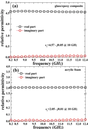
Fig. 1 shows the measured relative permittivity of glass/epoxy
composite (Fig. 1(a)) and the acrylic foam (Fig. 1(b)) at X- band and the permittivity at 10 GHz were 4.57−j0.05 and 2.05−j0.01, respectively.
To fabricate the resistive sheet, the conducting material was coated onto PI (polyimide) film purchased from SKC KOLON using film-coating equipment (KP-300, E&T Co., Ltd.). The sheet resistance of the resistive sheet was measured using a four-point probe. When fabricating the resistive sheet accord- ing to the design value, the sheet resistance of the resistive sheet was controlled by changing the coating conditions. Using the measurement data and possible ranges of the imple- mentable surface resistances, the modified Salisbury screen was designed.
3. DESIGN AND FABRICATION OF NAR- ROWBAND ABSORBER
First, narrowband-microwave absorber designed in the X- band is presented. To design the microwave absorber, the transmission line impedance equation [12] for a multilayer medium was derived. This is expressed as Eqs. (1) and (2) below,
(1)
(2)
Equation (1) gives the transformed surface impedance of the ground plane according to the layered media. Z
n+1, Z
nand Z
n-1are the surface impedance levels at the ground plane, β
nis the propagation constant of the n-th layer, and d
nis the thickness of the n-th layer. The calculated surface impedance (1) is inserted into Eq. (2), after which the reflection coefficient of the multi-layered absorber can be calculated. In Eq. (2), the Z
ois the free-space intrinsic impedance. When designing the nar- rowband absorber, Eqs. (1) and (2) were linked with a genetic algorithm (GA). The genetic algorithm used in this study repeatedly modifies a initially populated individual solutions.
At each step, the GA randomly selects individuals from the current population, and then they become parents and are used to reproduce the children for the next generation. With confined design parameter ranges, the population evolves toward an optimal solution. In this way, the reflection loss was optimized to satisfy −10 dB absorption in the X-band.
According to the design parameters at a specific frequency target, the resistive sheet variation was sensitive to the glass/
epoxy thickness while the foam layer was insensitive to mod- erate changes in the thickness of the glass/epoxy thickness.
When the thickness of the glass/epoxy composite becomes thinner, the operation principles of the proposed absorber become similar to those of a conventional Salisbury screen.
That is, as the thickness of the glass/epoxy composite decreases, Z
n 1+= Z
nZ
n 1–+ jZ
ntan ( β
nd
n)
Z
n+ jZ
n 1–tan ( β
nd
n) --- Γ = Z
n 1+– Z
0Z
n 1++ Z
0---
Fig. 1. The measured relative permittivity of (a) glass/epoxy com-
posite (GEP118) and (b) acrylic foam
the sheet resistance and foam layer thickness approaches the free-space impedance (377Ω) and λ/4 of the target frequency, respectively.
Because the glass/epoxy composite acts as a load-bearing structure, it should have a specific thickness. In this paper, the thickness of the glass/epoxy composite was set to be within 2.5 mm~3.0 mm by considering an implementable sheet resis- tance range. The final design values considering the imple- mentable physical parameters were 1.209 rad and 0.698 rad of the electrical length ( , n is refractive index, l is the thickness of dielectric, and λ
ois the free space wavelength) at the 9.5 GHz for the glass/epoxy and the acrylic foam, respec- tively, and 133 ohm/sq for the sheet resistance.
The absorbing performance of the designed absorber was checked using a full-wave simulator from CST Microwave Stu- dio. Fig. 2(b) shows the unit cell model with boundary con- ditions to check the absorbing performance of design values.
The free-space measurement method uses focusing lens to convert the spherical wave into plane wave. The converted plane wave becomes transverse electromagnetic (TEM) wave with respect to the specimen. If the size of the specimen is larger than 3λ × 3λ (λ is the wavelength), then the specimen seen by incident TEM wave seems to be semi-infinite plane.
The experimental environment can be simulated in the sim- ulator by using the boundary condition shown in Fig. 2(b). As shown in Fig. 2(b), the boundary condition (E
t= 0 and H
t= 0) was applied to the side-wall of absorber. When the boundary condition on the side-wall is applied, the absorber modeled in simulator is recognized as semi-infinite plane. Moreover, since the side-wall of the absorber is applied with the boundary con- dition of zero-tangential field, the excitation mode by the waveguide port is constrained to TEM mode. In this way, the experimental environment can be effectively simulated with almost no differences.
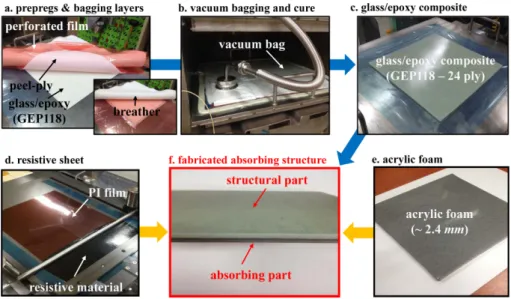
Using the design parameters, the glass/epoxy composite, resistive sheet, and foam layer were fabricated. Fig. 3 shows each fabricated layer and the final structure. First, the glass- fiber/epoxy composite structural part was fabricated through autoclave curing. To make the composite structural part, glass/
epoxy prepregs (GEP118) were used. Prepregs are fiber-glass fabrics that are pre-impregnated with epoxy resin for ease of processing and handling. 24 plies of glass/epoxy prepregs were layered by hand. After that, peel-ply, perforated release films, and breather were layered on the layered prepregs. The layered prepregs were vacuum-bagged and cured in an autoclave first for 30 min at 80
oC and then for 120 min at 130
oC. While the δ = 2πnl/λ
oFig. 2. (a) Geometry of the proposed microwave absorber, and (b) a unit cell model with boundary conditions to evalu- ate the absorbing performance of the designed absorber
Fig. 3. Fabrication process flow of the proposed microwave absorbing structure with glass/epoxy composite, resistive material, and
acrylic foam. Resistive sheet was fabricated using a film coater on the prepared PI film. To fabricate the glass/epoxy composite, 24
ply of glass/poxy prepregs were layered with curing accessories and cured in autoclave at 130
oC
specimen was being cured, the pressure was maintained at 6 atm. In the resistive sheet fabrication step, the carbon black based resistive material was coated on a PI film by using bar coater device. When coating the resistive material on the PI film, the printing conditions of bar coater were properly con- trolled to suit the material properties.
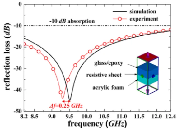
The reflection loss of the fabricated absorber was measured using the free-space measurement system introduced in the previous section to evaluate the microwave absorbing perfor- mance in the X-band. To allow a comparison of the reflection loss of the simulation with that of the experiment, two sets of values are shown together in the graph in Fig. 4. According to the measurement results, the fabricated absorber has a strong resonance at 9.25 GHz and reflection loss of −44 dB.
As shown in Fig. 4, the fabricated absorber showed excellent absorbing performance with a reflection loss of −10 dB absorption within the X-band. There is no significant differ- ence in the radar absorbing performance, and it was con- cluded that the proposed absorber with the desired radar absorbing performance could be designed and fabricated.
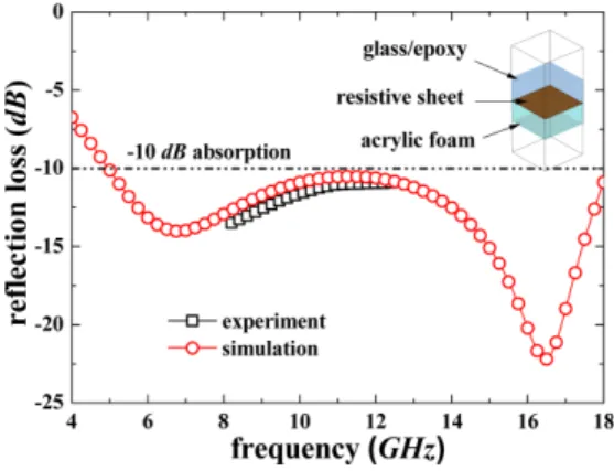
4. DESIGN AND FABRICATION OF BROADBAND ABSORBER
On the other hand, although the presented microwave absorbing structures have a lot of advantages to reduce the radar cross section, the absorbers used in stealth technology still have some disadvantages and limitations in terms of band- width. So far, frequency band of the microwave absorbing structures in the published papers was focused on X-band (8.2 GHz~12.4 GHz). The primary difficulties with radar absorbent and lossy materials are the skin effect, where elec- trical currents induced by an incident wave tend to concen- trate in the outer surface of a target. For the highly conductive materials like metal skins, the effective surface layer by skin effect is extremely thin for high frequencies, which acts excel- lent reflectors. However, absorbent materials are much less conductive to make much greater skin depth. As a result,
when the absorbent materials were designed at 10 GHz, it is ineffective against lower frequencies like 100 MHz or 1 GHz than target frequency due to the skin depth of the many mil- limeters or centimeters deep. In other words, an absorbers designed at a specific frequency has a resonance point which becomes the zero reactance and pure resistance. When fre- quency band is changed to the other frequency bands, match- ing point is deviated from the optimal design, as a result, the absorbing performance is greatly degraded.
For the broadband absorber, Eq. (3) was linked additively to the optimization code. Eq. (3) is an objective function which minimizes the reflection loss for the considered frequency ranges and reflectivity.
(3) OF = w
1i 1=
∑
n( R
r– R f ( )
i) + w
2i n 1= + n x+
∑ ( R
r– R f ( )
i) + w
3i n x 1= + +