• 검색 결과가 없습니다.

Study on the Nonlinear Characteristic Effects of Dielectric on Warpage of Flip Chip BGA Substrate

N/A
N/A
Protected

Academic year: 2021

Share "Study on the Nonlinear Characteristic Effects of Dielectric on Warpage of Flip Chip BGA Substrate"

Copied!
6
0
0

로드 중.... (전체 텍스트 보기)

전체 글

(1)

Study on the Nonlinear Characteristic Effects of Dielectric on Warpage of Flip Chip BGA Substrate

Seunghyun Cho

Department of Mechanical engineering, Dongyang Mirae University, Seoul 152-714, Korea (Received December 12, 2012: Corrected June 5, 2013: Accepted June 19, 2013)

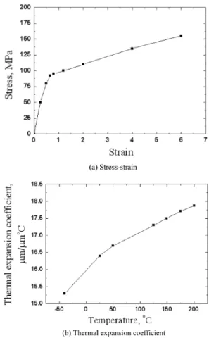
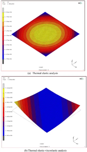
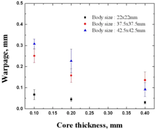
Abstract: In this study, both a finite element analysis and an experimental analysis are executed to investigate the mechanical characteristics of dielectric material effects on warpage. Also, viscoelastic material properties are measured by DMA and are considered in warpage simulation. A finite element analysis is done by using both thermal elastic analysis and a thermo-viscoelastic analysis to predict the nonlinear effects. For experimental study, specimens warpage of non- symmetric structure with body size of 22.5 ×22.5 mm, 37.5×37.5 mm and 42.5×42.5 mm are measured under the reflow temperature condition. From the analysis results, experimental warpage is not similar to FEA results using thermal elastic analysis but similar to FEA results using thermo-viscoelastic analysis. Also, its effect on substrate warpage is increased as core thickness is decreased and body size is getting larger. These FEA and the experimental results show that the nonlinear characteristics of dielectric material play an important role on substrate warpage. Therefore, it is strongly recommended that non-linear behavior characteristics of a dielectric material should be considered to control warpage of FCBGA substrate under conditions of geometry, structure and manufacturing process and so on.

Keywords: Nonlinear behavior, dielectric, warpage, FCBGA substrate, FEM

1. Introduction

High I/O interconnection density is becoming crucial in the high-end ICs like MPU, network systems, and chipset as I/O pad number is increased and package size is decreased at the same time.

1, 2)

So, the conventional packaging, such as wire- bonded lead-frame and ball grid array, may not be adapted to these high-end applications. The flip chip interconnection can provide solution for advanced packaging applications due to its advantages of large I/O number, enhanced thermal dissipation, and high electrical performance.

3)

In recent years, thin substrates have been developed to meet more requirements for high density interconnection and high electrical performance. Despite many technical challenges, ultra thin or coreless substrate has been studied for its capabilities for high-end flip-chip BGA (Ball Grid Array) applications.

4, 5)

Robert Sung compares the coreless (6 layers or 4 layers) and the standard (6 layers, 0.8 mm core layer) flip-chip substrate from the viewpoint of electrical performance.
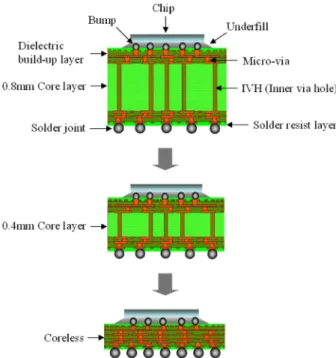
6)

Fig. 1 illustrates a schematic diagram of a conventional flip-chip BGA package for chipset application. A flip-chip

BGA package consists of a substrate, a chip, and their interconnection. The substrate has one core layer, 6 circuit layers, 4 dielectric build-up layers, and two solder resist layers. 6 circuit layers are connected electrically by micro- via and by an IVH. The interconnection consists of bumps with underfill. The bump connects electrically while underfill connects mechanically between the chip and substrate. As shown in Fig. 1, recently, the flip-chip BGA substrate core thickness has been decreased from 0.8 mm to below 0.4 mm for its shorter electrical path.

7)

Ultimately, a coreless substrate will be produced in the packaging industry.

However, the thin core or coreless flip-chip BGA substrate may be severely limited by substrate warpage since there are many mechanical challenges, such as coplanarity, underfill delamination and bump crack, caused by lower stiffness.

8, 9)

It is more difficult to control substrate warpage as core thickness is decreased. Also, it is not easy to predict thin substrate warpage by simulations. Although substrate warpage is strongly dependent on core thickness, the viscoelastic dielectric characteristics are more effective on warpage as core thickness is decreased.

Corresponding author

E-mail: [email protected]

© 2013, The Korean Microelectronics and Packaging Society

This is an Open-Access article distributed under the terms of the Creative Commons Attribution Non-Commercial License(http://creativecommons.org/

licenses/by-nc/3.0) which permits unrestricted non-commercial use, distribution, and reproduction in any medium, provided the original work is

properly cited.

(2)

Considering viscoelastic packaging materials, many researchers have studied the underfill (adhesive) film

10)

or the encapsulant.

11, 12)

In the substrate field, Kim has determined viscoelastic FR-4 substrate effects on microelectronics packaging reliability by considering temperature-dependent elastic and viscoelastic characteristics.

13)

Mauro Zarrelli et al. have studied viscoelastic characteristics of thermal setting resins in bi-material cantilever beam.

14)

The dielectric material nonlinear behavior characteristic effects for flip-chip BGA substrate are investigated by a finite element analysis and experiments. First of all, viscoelastic properties are measured by DMA and are considered in warpage simulation. Specimens are made to determine dielectric material warpage effects with a simple non- symmetric structure. They consist of a core layer, a copper layer, and two dielectric layers.

They are modeled and analyzed for computation by FEM software (MSC/MARC), a commercial simulation program.

15)

A finite element analysis is performed with two cases to investigate nonlinear characteristic effects. One is the thermal elastic analysis with temperature-dependent materials supplied by commercial data which is not considered viscoelastic characteristics. The other is the thermal elastic- viscoelastic analysis with temperature-dependent materials measured by experimental considering viscoelastic characteristics.

1.1. Experimental Methods

Fig. 2 shows a schematic structure of test specimen.

Upper side copper of CCL (Copper Clad Laminate) is etched away to maximize specimen warpage as the copper thickness difference between upper and lower sides is maximized. The dielectric build-up layers are laminated and pressed at high temperature. They are baked in the oven at a temperature of 180

o

C. Thus, initial warpage occurs when the specimen is pressed and baked during process. The dielectric layer and copper layer thicknesses are 0.0375 mm and 0.012 mm, respectively. Core layer thicknesses are 0.1 mm, 0.2 mm and 0.4 mm. The specimen has obviously shown viscoelastic dielectric material characteristics.

Fig. 3 shows temperature profile of reflow test. The maximum temperature peaks to 230

o

C within 2~3seconds and is decreased sharply. Temperature profile is a standard SMT (Surface Mounting Technology) reflow condition, used for the chip to package onto substrate. A reflow test equipment is used to understand dielectric warpage effects over the glass transition temperature (T

g

).

Viscoelastic characteristics of the dielectric is tested by DMA (TA instruments Q800) to determine storage (elastic) modulus, viscous (loss) modulus (G'') and damping coefficient (Tan ∆) as a function of temperature under 1 Hz using tension mode. DMA identifies transition regions in plastics, such as the glass transition, and may be used for quality control.

The specimens are carefully cut by CNC machine to prevent cutting defect. The size is at 2 mm×20 mm×0.0375 mm by IPC-TM-650 test methods manual (Number 2.4.24.4).

16)

Fig. 1. Schematic diagram of FCBGA package.

Fig. 3. Temperature profile of reflow test.

(3)

2. Finite Element analysis

The body size is 42.5 mm×42.5 mm with core thickness of 0.1 mm. Shell mesh is generated with condition that the elements and nodes are 3600 and 3721, respectively. A finite element modeling is determined by assuming the temperature conditions applied simultaneously to entire shell surface and one fixed surface point to the Z-direction to constrain the free body motion.

FEA is calculated by two dielectric material cases to verify nonlinear characteristics. One is the thermal elastic

analysis considering temperature-dependent material while the other is the thermal elastic-viscoelastic analysis.

The core layer is assumed to be orthotropic as a dielectric build-up layer while the copper layer is assumed to be isotropic. Temperature-dependent material properties are considered for all component materials through FEA. Fig.

4(a)-(c) show core layer temperature-dependent properties. Fig.

5(a)-(b) present temperature-dependent dielectric properties.

Also, the electroplated copper elastic modulus and Poisson’s ratio are, respectively, 30 GPa and 0.343. The stress-strain curve and thermal expansion coefficient are shown in Figs.

6 (a), (b).

Fig. 4. Properties of the core material.

Fig. 5. Properties of dielectric. Fig. 6. Mechanical and thermal properties of the copper.

(4)

seconds. The storage modulus as a function of temperature is input as an elastic modulus in warpage simulation.

Fig. 8 shows the dielectric storage and loss modulus’s under constant temperature of 30

o

C in DMA test. The specimen is pulled at 20 um under constant drive force of 1.03 N and frequency of 1 Hz in DMA test. Storage modulus steeply decreases from initial 4.3 GPa to 4.22 GPa after 40 minutes and gradually is increased to 4.24 GPa after 100 minutes. As shown in figure 8, the storage modulus is little changed under low temperature of 30

o

C while the loss modulus is very low.

3.2. Warpage simulation

Fig. 9(a), (b) show warpage specimen distributions by FEM after the reflow test. The specimen has 0.1 mm core thickness and the reflow test condition is shown in Fig. 3.

Fig. 9(a) is the result of thermal elastic analysis while Fig.

9(b) is the result of thermal elastic-viscoelastic analysis.

Warpage occurs at four corners in the specimen simultaneously during reflow test and disappears nearly to 0.18 mm after the reflow test. In addition, a thermal elastic analysis of reflow does consider the temperature-dependent material as illustrated in Fig. 9(a). However, the counter specimen corners are rolled up after the reflow test considers nonlinear dielectric characteristics as shown in Fig. 9(b). The specimen warpage is about 9.6 mm.

Fig. 10 shows specimen warpage distributions during the reflow test. The specimen sizes are set at 22.0 mm×22.0 mm, 37.5 mm×37.5 mm, and 42.5 mm×42.5 mm, respectively.

Core layer thickness is same at 0.1 mm. Specimen warpage reaches peak at 20.6 mm, 11.1 mm, 8.6 mm, respectively, at 350 seconds during reflow. Warpage is decreased to 9.6 mm, 4.9 mm and 3.5 mm after the end of reflow. Residual warpages occur mainly by the nonlinear characteristics of dielectric since residual specimen warpage occurs little in Fig. 7. Storage modulus of dielectric material in DMA test.

Fig. 8. Dielectric storage modulus and loss modulus under constant temperature of 30

o

C in DMA test.

Fig. 9. Warpage distributions of the specimen with body size

42.5 mm ×42.5 mm after reflow test.

(5)

thermal elastic analysis when only temperature-dependent properties are considered as mentioned in Figure 9(a).

Nonlinear characteristics have been considered to understand the substrate warpage as yet since substrate has the thick core layer to reduce warpage. The core layer strongly influences warpage. On the other hand, nonlinear dielectric characteristics are considered more important as core thickness is decreased, specially, in coreless substrate.

Thus, the simulation results mean that nonlinear characteristics should be considered to understand substrate or package warpages in the future.

3.3. Warpage test

Fig. 11 shows the average and standard variation of specimen warpage before the reflow test. These results are initial warpages. Ten specimens are prepared for measure- ment. As illustrated in Fig. 12, the average warpages with body size of 22 mm×22 mm increase slowly from 0.04 mm to 0.07 mm as core thickness decreases. On the other hand, average warpage is increased steadily as core thickness is decreased from both the body sizes of 37.5 mm×37.5 mm

and 42.5 mm×42.5 mm. These initial warpages occur by baking process to cure dielectric build-up layers of non- symmetric structure in Figure 2.

Fig. 12 shows the average and standard warpage variation after the reflow. The average warpage difference among specimens with core thickness of 0.4 mm is small for body sizes.

In case of the 22×22 mm body size, the average warpages with core thicknesses of 0.4 mm, 0.2 mm, and 0.1 mm are 0.04 mm, 0.34 mm, and 1.7 mm, respectively. In case of the 37.5 ×37.5 mm body size, the average warpages with the same core thicknesses for the 22×22 mm body size are 0.2 mm, 2 mm and 5.7 mm, respectively. Also, the average warpage with body size of 42.5×42.5 mm is 0.14 mm, 2.6 mm and 7.2 mm with the same core thicknesses, respectively.

The warpage is sharply increased as core thickness is decreased with the body size increase. The results present a significant dielectric material effects of the nonlinear characteristics on the substrate warpage. Thus, it is very important to understand the nonlinear characteristics to reduce warpage to meet trends of thin and large substrates.

Fig. 13 shows warpage distributions after the reflow. As shown in Figure 14, there is a distinct shape deformation.

This occurs at counterpart corner of specimen such that Fig. 10. Warpage distributions of the specimen during reflow test.

Fig. 11. Specimens’ warpage before reflow test.

Fig. 12. Specimen’s warpage after reflow test.

Fig. 13. Specimen’s warpage distributions after reflow.

(6)

4. Conclusions

The specimens with the non-symmetric structure are analyzed by the FEM analyses and the experimental analyses to understand the nonlinear characteristics of dielectric effects on warpage. Computed analysis results show that warpage pattern is different between the thermal elastic analysis and thermal elastic- viscoelastic analysis.

The specimen’s counter corner is rolled up, and it is explinaed by the material nonlinearity from the FEA calculations. However, in the thermal elastic analysis, the warpage occurs at the four corners of the specimen simultaneously, and little remains after the reflow test. Also, the warpage specimen pattern after the reflow is different from the conventional researches. . The nonlinear effect on warpage is increased more in thin built-up structure. They are suppressed by the thick core layer and are disclosed as the core thickness is decreased. The warpage pattern distinctly increases as the specimens’ body sizes grow large.

Although the FEA and the experimental results show similar warpage shape pattern, the numerical magnitudes of the warpage differ from each other. Thus, it is strongly recommended that more precise nonlinear characteristics of the dielectric material should be considered in the FEA as substrate thickness is decreased in the future.

Acknowledgments

This work was supported by the 2011 Research Founda- tion of Dongyang Mirae University

References

1. Ming-Yi Tsai, C.H.Jeter and T.Otto Wang, “Investigation of Thermomechanical Behaviors of Flip Chip BGA Packages

S. Hsiao, “Advantage and challenge of coreless Flip-chip BGA Microsystems”, IMPACT . 346 (2007).

5. Chiu Christine, Chang K. C., Wang Jones, Lee C. H, Shen Kedy and Wang Leonardo, “Challenges of thin core substrate Flip Chip package on advanced Si Nodes”, ECTC '07. Pro- ceedings. 57

th

. 22 (2007).

6. Robert Sung, Kevin Chiang, Y. P. Wang and C. S. Hsiao,

“Comparative analysis of electrical Performance on coreless and standard Flip-Chip Substrate”, ECTC '07. Proceedings.

57

th

, 1921 (2007).

7. Seunghyun Cho, Soonjin Cho and Joseph Y. Lee, “Estimation of warpage and thermal stress of IVHs in flip–chip ball grid arrays package by FEM”, Microelectron Reliab, 48, 300 (2008).

8. Masazumi Amagai, “Characterization of chip scale package materials”, Microelectron reliab, 39, 1365 (1999).

9. John H. Lau and W. –W. Ricky Lee, “Effects of Build-Up Printed Circuit Board Thickness in the Solder Joint Reliability of a Wafer Level Chip Scale Package(WLCSP)”, Transaction on Components and Packaging Technologies, 25(1), 3 (2002).

10. Man-Lung Sham, Jang-Kyo Kim and Joo-Hyuk Park,

“Numerical analysis of plastic encapsulated electronic pack- age reliability: Viscoelastic properties of underfill resin”, Computational Materials Science, 40, 81 (2007).

11. Masazumi Amagai, “Characterization of chip scale package materials”, Microelectron reliab, 39, 1365 (1999).

12. Xiong, Z. and Tay A. A. O., “Modeling of viscoelastic effects on interfacial delamination in IC packages”, ECTC '00. Pro- ceedings. 50

th

, 1326 (2000).

13. Y. K. Kim, “Viscoelastic Effect of FR-4 Material on Packag- ing Stress Development”, IEEE Transactions on Advanced Packaging, 30(3), 411 (2007).

14. Mauro Zarrelli, Ivana K. Partridge and A. D. Amore,

“Warpage induced in bi-material specimens : Coefficient of thermal expansion, chemical shringkage and viscoelastic modulus evolution during cure”, Composites: Part A, 37, 565 (2006).

15. MSC. Marc User’s Manual. MSC.software corporation.

(2005).

16. IPC-TM-650 test methods by the manual(Number 2.4.24.4).

17. F. Tanaka and S. F. Edwards, “Viscoelastic properties of phys- ically crosslinked networks (part II) : Dynamic moduli, J.

Non-Newt”, Fluid Mech, 43(1-2), 273 (1992).

수치

Fig. 3 shows temperature profile of reflow test. The maximum temperature peaks to 230 o C within 2~3seconds and is decreased sharply
Fig. 5. Properties of dielectric. Fig. 6. Mechanical and thermal properties of the copper.
Fig. 8 shows the dielectric storage and loss modulus’s under constant temperature of 30 o C in DMA test
Fig. 13 shows warpage distributions after the reflow. As shown in Figure 14, there is a distinct shape deformation.

참조

관련 문서

The effects of recycling on the tensile bond strength of new and clinically used stainless steel orthodontic brackets: an in vitro study. Material testing of

This study was conducted to investigate the effects of 12 weeks after school physical activity program on body composition and PAPS in obese elementary

Objectives : The purpose of this study was to investigate the effects of general characteristics, health characteristics, mental health characteristics, suicidal

Evaluating parameters of osseointegrated dental implants using finite element analysis-a two- dimentional comparative study examining the effects of implant

In an effort to develop a new method to remove nitrogen, this study examined the effects of C/N ratio, carbon source and nitrogen concentration on

The purpose of study are analyzing the effects of dance majors' self-management on dance performance ability, self-efficacy and concentration, In the future,

The purpose of this study was to investigate the effects of sound-finding strategies based on phonological awareness on word recognition, oral reading

The purpose of this study was to investigate the effects of 8 weeks trampoline exercise on health promotion (health related fitness, blood lipid) in