374
†Corresponding author
E-Mail : [email protected] (S. -S. Park)
Effects of Chamber Pressure on Dielectric Properties of Sputtered MgTiO
3Films for Multilayer Ceramic Capacitors
Sang-Shik Park
†School of Nano & Materials Engineering, Kyungpook National University, Kyungpook 742-711, Korea (Received June 29, 2010 : Received in revised form July 10, 2010 : Accepted July 19, 2010)
Abstract
MgTiO3 thin films were prepared by r.f. magnetron sputtering in order to prepare miniaturized NPO type MLCCs.MgTiO3 films showed a polycrystalline structure of ilmenite characterized by the appearance of (110) and (202) peaks. The intensity of the peaks decreased with an increase in the chamber pressure due to the decrease of crystallinity which resulted from the decrease of kinetic energy of the sputtered atoms. The films annealed at 600oC for 60min. showed a fine grained microstructure without micro-cracks. The grain size and roughness of the MgTiO3 films decreased with the increase of chamber pressure. The average surface roughness was 1.425~0.313 nm for MgTiO3 films prepared at 10~70 mTorr. MgTiO3 films showed a dielectric constant of 17~19.7 and a dissipation factor of 2.1~4.9% at 1MHz. The dielectric constant of the films is similar to that of bulk ceramics. The dielectric constant and the dissipation factor decreased with the increase of the chamber pressure due to the decrease of grain size and crystallinity. The leakage current density was 10−5~10−7A/cm2 at 200kV/cm and this value decreased with the increase of the chamber pressure. The small grain size and smooth surface microstructure of the films deposited at high chamber pressure resulted in a low leakage current density. MgTiO3 films showed a near zero temperature coefficient and satisfied the specifications for NPO type materials. The dielectric properties of the MgTiO3 thin films prepared by sputtering suggest the feasibility of their application for MLCCs.
Key words
MgTiO3 films, MLCC, capacitance, leakage current.1. Introduction
Magnesium titanate based materials are extensively used as a dielectric of NPO type multilayer ceramic capacitors (MLCCs), which have been widely used in electric and electronic devices. It is known that MgTiO
3bulk ceramics exhibit a low dielectric loss, a near zero temperature coef- ficient and dielectric constant of the range of 17~20 in microwave frequencies.
1,2)The recent developments in MLCC fabrication technology have focused on the improve- ment of volumetric efficiency, cost reduction, improvement in reliability, and the design of new products with im- proved performance.
3-5)Especially, with the recent tendency in miniaturization of electronic equipments, MLCCs are required to have a high electrostatic capacitance and also to be miniaturized. For enhancing of the electrostatic cap- acitance of MLCCs, one of the most effective means is to provide a thin dielectric layer between the inner elec- trodes. The capacitance of the MLCC is expressed by the following equation.
C = N ( ε
0· ε
r· A ) / d (1)
Where, C is capacitance, N layer number, ε
0permittivity
in vacuum, ε
rdielectric constant of ceramic film, A the surface area of electrode, and d thickness of dielectrics.
Therefore, in the capacitor of equivalent size, the increase of capacitance can be obtained by increase of ε
rand N and decrease of d.
The dielectric sheets of MLCCs have been formed by die coater and lip coater and thickness of dielectric sheets has been decreased to about 1 µm levels.
6)However, because the preparation of thinner dielectric layers by casting method such as die coater and lip coater is very difficult, it is needed to consider new method except casting method.
The development of thin film capacitors designed by thin film technologies have been required for next generation capacitors.
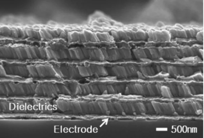
7,8)Vapor deposition processes have inherent advantages over traditional MLCC technology, such as the ability to deposit very thin, uniform and defect free dielectric sheets. Our recent works showed that MLCCs could be manufactured by thin film technology. Fig. 1 shows a SEM cross-section image of MLCC prepared by e-beam evaporation using a shadow mask. Alternating dielectric and electrode layers can be prepared through the x and z-axis movement of shadow mask.
9)Although MgTiO
3films have been studied for appli-
cation in microwave devices, the studies for MLCCs is
very uncommon. In this work, MgTiO
3films were de-
posited using R.F. magnetron sputtering technique. The
aim of this study is to evaluate the effects of deposition pressure on dielectric properties of MgTiO
3films. Also, the relationships between microstructure and dielectric properties of films were investigated.
2. Experimental Procedure
MgTiO
3thin films were deposited on p-Si(100) substrate using a conventional r.f. magnetron sputtering system.
MgTiO
3ceramic target was prepared by conventional sintering methods from high purity(> 99.9%) MgO and TiO
2powders. After working chamber was pumped down to 1 × 10
−6Torr, sputtering gas mixture (Ar:O
2= 1:1) was injected and then, MgTiO
3films were deposited at various pressure of 10 mTorr to 70 mTorr. The target was pre- sputtered for 10 min. to eliminate contamination of target and maintain homogeneity of target composition. The de- tailed deposition conditions were described in Table 1. The crystal structure of the films was determined by X-ray diffraction (XRD, Panalytical X’pert pro) employing Cu k α radiation and Ni filter. The microstructure and composition of MgTiO
3films were determined using scanning electron microscopy and energy dispersive x-ray spectroscopy (SEM-EDX, Jeol JSM-6700F) and The roughness of each film was measured with atomic force microscopy (AFM, Park system XE-100). For the electrical measurement, plat- inum top electrode with 100 nm thickness and 100 µm
diameter were deposited using dc sputtering, that is, metal- insulator-metal (MIM) capacitors with a Pt/MgTiO
3/Pt/TiO
2/ Si structure were fabricated. The dielectric constant and dissipation factor as a function of frequency were measured using an impedance-gain phase analyzer (Hewlett-Packard 4194A). The current-voltage (I-V) measurements were per- formed with a picoammeter (Hewlett-Packard 4140B) under conditions of a 0.1V voltage step and a delay time of 0.1s.
3. Results and Discussion
Fig. 2 shows XRD patterns of the MgTiO
3films an- nealed at 600
oC after deposited using r.f. power of 200W.
XRD patterns indicated that MgTiO
3films showed a poly- crystalline structure of the ilmenite characterized by the appearance of (110) and (202) peaks. The intensity of peaks decreased with increasing the chamber pressure and the (110) and (202) peaks disappeared at 50 and 70 mTorr.
In general, the sputtered atoms show the reduction of surface mobility on substrate surface with the increase of chamber pressure. Therefore, the decrease of peak intensity is probably due to decrease of crystallinity which resulted from decrease of kinetic energy of the sputtered atoms.
Fig. 3 shows SEM surface images of MgTiO
3films deposited on Si(100) substrate as a function of chamber pressure. The films were annealed at 600
oC for 60min.
The surface microstructures revealed that MgTiO
3films had a fine grained microstructure without micro-cracks.
The SEM images indicated that grain size decreased with increasing the chamber pressure. The decrease of grain size with chamber pressure is due to that high chamber pressure decreases mean free path of sputtered particles, resulting in a decrease of the kinetic energy of arriving atoms.
10)Accordingly, it is inferred that the small grain size at high chamber pressure is attributed to atoms with
Fig. 1. SEM cross-section image of multilayer capacitor with BaTiO3and Al alternating layers.9)
Table 1. Preparation conditions of MgTiO3 thin films.
Parameters Conditions
Target-substrate distance Substrate
Ar:O2 R.f. power Base pressure Working pressure Substrate temperature
60 mm
p-Si(100), Pt/TiO2/Si 1:1
200 W 5× 10⁻⁶Torr 10~70mTorr Room temp.
Fig. 2. XRD patterns of MgTiO3 films as a function of chamber pressure.
low kinetic energy.
Fig. 4 shows deposition rate for MgTiO
3thin films of Fig. 2. The deposition rate of films was remarkably de- creased with increasing a chamber pressure. The deposition rate of films revealed 3.05, 2.14, 0.625 and 0.373 nm/min at chamber pressure of 10, 30, 50 and 70 mTorr, respect- ively. The calculated mean free path at 10 mTorr was 7.2 times of that at 70 mTorr. Because deposition rate is directly related to mean free path, the decrease of deposition rate is due to the increase of scattering from the gas atoms.
It is important to investigate the surface morphology of
MgTiO
3films, since the surface morphology will affect the electrical properties of films. The influences of chamber pressure on the morphologies of MgTiO
3films were examined by AFM. Fig. 5 shows three dimensional AFM images of MgTiO
3films. The average roughness of films decreased with increasing the chamber pressure. The average surface roughness was 1.425, 1.408, 0.689 and 0.313 nm for MgTiO
3films prepared at 10, 30, 50, 70 mTorr, respect- ively. Because of atomic shadowing effects, the surface roughness can increase with film thickness. However, the similar roughness tendency was shown in films with similar thickness prepared by controlling the deposition time.
These results imply that in the case of low deposition rate at a high pressure, newly arrived atoms have more sufficient time to relax to low energy configurations, leading to the formation of smoother films.
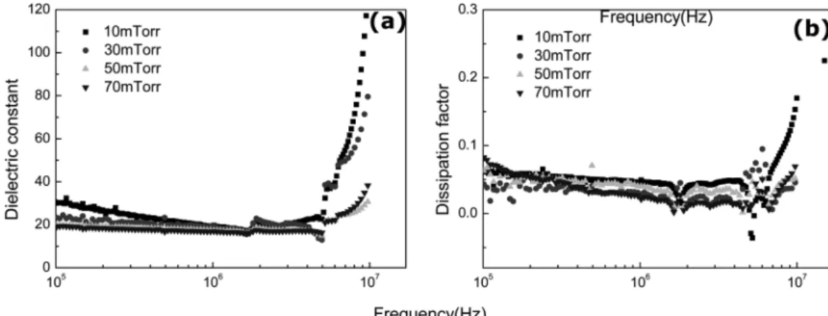
11)Fig. 6 shows the variation of dielectric constant and dissipation factor (tan δ) as a function of frequency for MgTiO
3films deposited at various chamber pressures.
The dielectric constant and dissipation factor of MgTiO
3films exhibited little dispersion at the high frequencies up to 5MHz. The dielectric constant at a frequency range of 100kHz to 10MHz decreased with increasing the chamber pressure. The decrease of dielectric constant with chamber pressure is attributed to the decrease in grain size of the MgTiO
3films. The dielectric constant of films deposited at various chamber pressures were 19.7 to 17 at 1MHz.
The dielectric constant of the films is similar to that of
Fig. 3. SEM surface morphologies of MgTiO3 films; (a) 10mTorr, (b) 30mTorr, (c) 50mTorr and (d) 70mTorr.Fig. 4. Variation of deposition rate of MgTiO3 films prepared under various chamber pressures.
related to surface morphology. The structural disorder of MgTiO
3films prepared by r.f. magnetron sputtering may affects the large dissipation factor.
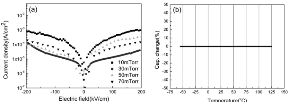
The leakage current in MLCCs should be as low as
~2 × 10 A/cm at 200kV/cm. Fig. 7(b) shows capacitance vs. temperature property of MgTiO
3films. For the NPO type dielectrics, the capacitance must not change by more than ± 30ppm/°C from the value at 25
oC over the tem-
Fig. 5. AFM surface morphologies of MgTiO3 films; (a) 10mTorr, (b) 30mTorr, (c) 50mTorr and (d) 70mTorr.
Fig. 6. (a) Dielectric constant and (b) dissipation factor of MgTiO3 films as a function of frequency.
perature range –55 to 125
oC. MgTiO
3films show a near zero temperature coefficient. The capacitance change with operating temperature satisfied the specification for NPO type materials.
4. Conclusion
The application of MgTiO
3thin films for NPO type MLCCs was proposed in this study. MgTiO
3thin films were prepared by r.f. magnetron sputtering. Particularly, the relationships between chamber pressure and dielectric properties of films were investigated. The grain size and roughness of MgTiO
3films decreased with an increase of chamber pressure due to short mean free path and low de- position rate. The grain size and roughness of films influ- ences dielectric constant, dissipation factor and leakage current. The dielectric constant and dissipation factor of MgTiO
3films obtained by sputtering are 17~19.7 and 4.9~
2.1% at 1MHz, respectively and are comparable to that by other deposition methods. Leakage current density is about 8 × 10
−6~ 2 × 10
−7A/cm
2at 200kV/cm. These results suggest the feasibility that the miniaturized NPO type MLCCs can be prepared by R.F. magnetron sputtering.
Acknowledgement
This work was supported by the Kyungpook National University Research Grant, 2008.
References
1. Y. Jiang, R. Guo and A. S. Bhalla, J. Phys. Chem. Solids, 59, 611 (1998).
2. M. P. Baura-Pena, M. J. Martinez-Lope and M. E.
Garcia-Clarel, J. Mater. Sci., 26, 4341 (1991).
3. T. Nomura, N. Kawano, J. Yamamatsu and T. Arashi, Jpn.
J. Appl. Phys., 34, 5389 (1995).
4. Y. Okino, H. Sizuno, S. Kusumi and H. Kisi, Jpn. J.
Appl. Phys., 33, 5393 (1994).
5. J. Yamamatsu, N. Kawano, T. Arashi, A. Sato, Y. Nakano and T. Nomura, J. Power Sources., 60, 199 (1996).
6 . Y. S a k a b e , Y. Ta k e s h i m a a n d K . Ta n a k a , J . Electroceram., 3, 115 (1999).
7. R. Xu, M. Shen, S. Ge, Z. Gan and W. Cao, Thin Solid Films, 406, 113 (2002).
8. Y. Takeshima, T. Tanaka and Y. Sakabe, J. Am. Ceram.
Soc., 106, 441 (2000).
9. S. Park, Integrated Ferroelectrics, 74, 87 (2005) 10. L. T. Lamont and A. Lange, J. Vac. Sci. Technol., 7, 198
(1970).
11. Y. Zhao, Y. Qian, W. Yu and Z. Chen, Thin Solid Films, 286, 45 (2002).
12. J. Bernard, D. Hpuivet, J. El Fallah and J. M. Haussonne, J. Eur. Ceram. Soc., 24, 1877 (2004).
13. K. Wakino, Ferroelectrics, 91, 69 (1989).
14. Y. H. Choi and J. Lee, Thin Solid Films, 385, 43 (2001).
15. V. M. Ferreira, J. L. Baptista, S. Kamba and J. Petzelt, J.
Mater. Sci., 28, 5894 (1993).
Fig. 7. (a) Leakage current and (b) capacitance change with temperature of MgTiO3 films.