Kor. J. Mater. Res.
Vol. 24, No. 4 (2014)
207
Effects of Sputtering Pressure on the Properties of BaTiO 3 Films for High Energy Density Capacitors
Sangshik Park †
School of Nano Materials Engineering, Kyungpook National University, Gyeongsang-daero 2559, Sangju, Gyeongbuk 742-711, Korea
(Received February 6, 2014 : Received in revised form April 8, 2014 : Accepted April 9, 2014)
Abstract
Flexible BaTiO3 films as dielectric materials for high energy density capacitors were deposited on polyethylene terephthalate (PET) substrates by r.f. magnetron sputtering. The growth behavior, microstructure and electrical properties of the flexible BaTiO3 films were dependent on the sputtering pressure during sputtering. The RMS roughness and crystallite size of the BaTiO3 increased with increasing sputtering pressure. All BaTiO3 films had an amorphous structure, regardless of the sputtering pressures, due to the low PET substrate temperature. The composition of films showed an atomic ratio (Ba:Ti:O) of 0.9:1.1:3. The electrical properties of the BaTiO3 films were affected by the microstructure and roughness. The BaTiO3 films prepared at 100 mTorr exhibited a dielectric constant of ~80 at 1 kHz and a leakage current of 10−8A at 400 kV/cm. Also, films showed polarization of 8µC/cm2 at 100 kV/cm and remnant polarization (Pr) of 2µC/cm2. This suggests that sputter deposited flexible BaTiO3 films are a promising dielectric that can be used in high energy density capacitors owing to their high dielectric constant, low leakage current and stable preparation by sputtering.Key words
flexible BaTiO3 film, sputter, high energy density capacitor, dielectric constant, leakage current.1. Introduction
Pulsed power systems and directed energy weapons, such as electromagnetic and electrothermal guns, require high energy density capacitors. The main limitation to improving capacitors in these systems by delivering more energy is the capacitance of the energy storage capacitor themselves. Dielectric materials play a key role in power capacitors for charge control and energy storage.
1-3)Polymer dielectrics are currently the primary choice of materials for high energy density capacitors owing to their relatively high breakdown strength, low dielectric loss and low cost. The polymers in commercial power capacitors include polyethylene terephthalate(PET), poly- carbonate(PC), polypropylene(PP), etc.
4-6)but the low dielectric constant( ε
r~ 2 to 3) of polymer dielectrics limits their applications. On the other hand, ceramic capacitors have a much higher energy density than polymer film capacitors due to the high dielectric constant of ceramics.
However, ceramic capacitors exhibit low breakdown strength due to microstructural defects, which results in a
low energy density.
7,8)The energy that can be stored in a capacitor depends on the relative dielectric constant and the square of the breakdown strength of the dielectric layer according to equation (1)
E = 1/2· ε
o· ε
r·E
b2(1)
where E is the energy stored per unit volume(J/m
3), ε
ois the dielectric constant of a vacuum, ε
ris relative dielectric constant of the dielectric film and E
bis the breakdown strength(V/m). The energy density of a capacitor will increase if E
bis kept constant and the ε
rvalue is increased.
The aim of this study was to prepare a ceramic dielectric film for high energy density capacitors with the structure of a polymer film capacitor. In this study, barium titanate(BaTiO
3) films were deposited on an aluminum metallized PET substrate. BaTiO
3has been evaluated extensively for electronic applications including MLCC, high energy capacitors and resistor.
9-11)Because
†
Corresponding author
E-Mail : [email protected] (S. Park, Kyungpook Nat'l Univ.)
© Materials Research Society of Korea, All rights reserved.
This is an Open-Access article distributed under the terms of the Creative Commons Attribution Non-Commercial License (http://creative-
commons.org/licenses/by-nc/3.0) which permits unrestricted non-commercial use, distribution, and reproduction in any medium, provided the
original work is properly cited.
of its relatively high dielectric constant(150~6,000), BaTiO
3is considered a potential dielectric material for high energy density capacitor applications.
10)A range of techniques have been used to prepare BaTiO
3thin films, including sputtering,
12)chemical vapor deposition,
13)pulsed laser deposition
14)and sol-gel techniques.
15)In this study, BaTiO
3films were deposited on flexible PET substrates by r.f. magnetron sputtering for roll to roll process. The applicability of a BaTiO
3/PET film to high energy density capacitors was evaluated by examining the effects of the sputtering pressure on the electrical properties.
2. Experimental procedure
The flexible BaTiO
3films were deposited on PET sub- strates at room temperature by r.f. magnetron sputtering.
A 2 inch diameter BaTiO
3target(Cerac Inc.) was used.
Deposition was performed at a fixed substrate to target distance of 60 mm. PET films, 4~10 µm in thickness, were used as main substrates and also BaTiO
3films were deposited on Si wafer to examine the phase formation after annealing. The base pressure was < 1 × 10
−6Torr and sputtering was carried out in an Ar atmosphere. The target was pre-sputtered for 30 min. before depositing the BaTiO
3films to remove surface contamination and non- stoichiometry of the BaTiO
3target. A r.f. power of
200 W was applied to the target, and BaTiO
3films were deposited on PET and Al/PET substrates. BaTiO
3films were prepared at different sputtering pressures(30 to 100 mTorr) as a sputtering parameter. The thickness of the BaTiO
3films was controlled by the deposition time. The thickness and surface morphology of the flexible BaTiO
3films were measured by field effect scanning electron microscopy(FESEM) and atomic force microscopy(AFM).
The structural properties and chemical state of the BaTiO
3films were examined by X-ray diffraction(XRD) and X- ray photoelectron spectroscopy(XPS), respectively. To measure the electrical properties of the BaTiO
3films, Al top electrodes, 100 nm in thickness and 0.1-1 mm in diameter, were deposited by dc sputtering, and capacitors with an Al/ BaTiO
3/Al/PET structure were fabricated.
The dielectric constant and dissipation factor were mea- sured as a function of frequency using an impedance-gain phase analyzer. The current-voltage(I-V) measurements were performed using a picoammeter, and the polarization- electric field(P-E) curves were measured using a ferro- electric test system.
3. Results and discussion
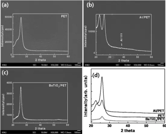
Fig. 1 shows SEM surface images of PET, Al/PET and BaTiO
3/PET, as well as the XRD patterns of these samples. The microstructure of the PET substrates (Fig.
Fig. 1. SEM images and XRD patterns of (a) PET, (b) Al/PET, (c) BaTiO
3/PET and (d) XRD patterns of (a) (c) samples.
1(a)) is the typical surface morphology produced during the manufacture of biaxially-oriented PET films. The peak in the range, 20~30
o, was assigned to the semi-crystalline structure of PET.
6)Fig. 1(b) shows the surface images of an Al film deposited on PET. The Al film was deposited as a bottom electrode material. The Al surface was com- posed of indistinct, small crystallites due to the low thickness of approximately 50 nm, and showed a cry- stalline(111) peak at 38.3
o. Fig. 1(c) shows images of the BaTiO
3film deposited on PET. The BaTiO
3film with a 910 nm thickness did not show any grain morphology.
XRD showed the peak only for the PET substrate. This suggests that the BaTiO
3film has a nano-crystalline or
amorphous structure. The XRD patterns of (a) to (c) were re-plotted on same scale to compare the peak intensities of the samples. The intensity of the main peak for PET at 25.8
odecreased considerably with increasing the thickness of the coating layer, such as Al and BaTiO
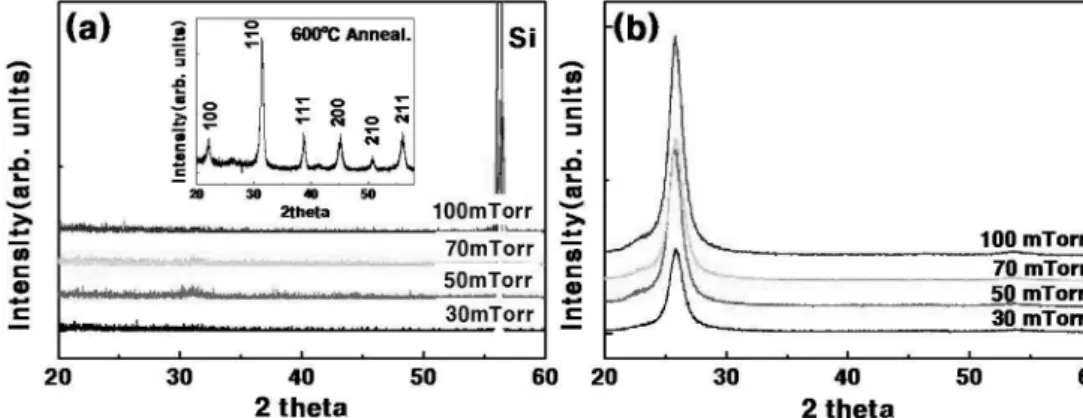
3. Fig. 2 shows XRD patterns of the BaTiO
3films de- posited at room temperature as a function of the sput- tering pressures. The sputtering pressure was controlled by the argon gas flow rate used as the sputtering gas.
BaTiO
3films were deposited on two types of substrates, Si and PET, to compare the substrate dependence on film growth. The BaTiO
3films deposited on a Si substrate in Fig. 2(a) did not show any crystalline peak. When the
Fig. 2. XRD patterns of BaTiO
3films deposited on (a) Si and (b) PET substrates at a range of sputtering pressures.
Fig. 3. SEM surface images of BaTiO
3films deposited on PET substrates at (a) 30 mTorr and (b) 100 mTorr and (c) deposition rate and
(d) RMS roughness obtained by AFM as a function of the sputtering pressure.
BaTiO
3films deposited on Si were annealed at 600
oC, the films transformed to a crystalline phase. This result means that the composition of BaTiO
3films deposited at room temperature is similar to that of target. Fig. 2(b) shows XRD patterns of the films deposited on PET. All XRD patterns of the BaTiO
3films showed only an intense PET substrate peak at 25.8
o. All BaTiO
3films showed an amorphous structure regardless of the sput- tering pressure and substrates used due to the low substrate temperature. BaTiO
3films deposited under 500
o
C have been reported to be amorphous.
12,16,17)Fig. 3(a) and (b) show SEM surface images of the BaTiO
3films grown on PET substrates under 30 and 100 mTorr, respectively. The surface of all BaTiO
3films deposited at pressures from 30 to 100 mTorr was relatively smooth without defects, such as cracks and pinholes due to deposition at low temperatures. All films showed a featureless morphology with a typical amorphous struc- ture. Fig. 3(c) shows the deposition rate as a function of the sputtering pressure. The deposition rate of the films decreased with increasing sputtering pressure due to the decrease in mean free path.
18,19)The deposition rate of the films deposited at 30 and 100 mTorr was 14.2 and 9.1 nm/min, respectively. The decrease in deposition rate with increasing pressure was attributed to collision scat- tering between the sputtered BaTiO
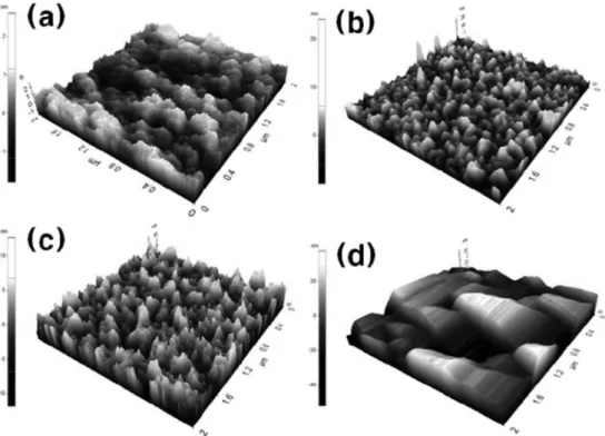
3and Ar species in the chamber. Fig. 3(d) shows the surface RMS roughness of the films obtained by AFM as a function of the sputtering pressure. As shown in the AFM images in Fig.
4, the RMS roughness of the films increased with increasing sputtering pressure. The BaTiO
3films showed a RMS roughness of 0.6 to 10.6 nm at a pressure of 30 to 100 mTorr. This can be understood by the following mechanism. The energy of the particles decreased with increasing pressure because of the higher number of collisions.
20)The surface mobility of the particles de- creased with decreasing energy, and the coalescence of the crystals was limited.
21)Fig. 4 shows AFM images of BaTiO
3films deposited on PET at different sputtering pressures. The surface roughness of the films increased with increasing sput- tering pressure. A uniform and crack-free surface mor- phology was observed for all specimens investigated. On the other hand, the films deposited at 100 mTorr showed a very different morphology and large crystallites, which is in contrast to the films deposited at 30~70 mTorr. The increase in crystallite size can be explained by the relationship between the mean free path, λ(cm), and the sputtering pressure as follows:
λ = 2.33 × 10
−20T/(P δ
m2) (2) where T(K) is the temperature, P(Pa) is the pressure and δ
m(cm) is the molecular diameter.
22)From Eq. (2), the sputtered atoms undergo a large number of collisions when the sputtering pressure is high and have a higher probability of agglomeration. Therefore, the crystallite size can increase before arriving at the
Fig. 4. AFM images of BaTiO
3films as a function of the sputtering pressure; (a) 30 mTorr, (b) 50 mTorr, (c) 70 mTorr and (d) 100 mTorr.
substrate surface. On the other hand, no signals corres- ponding to crystalline BaTiO
3films could be observed from the XRD patterns in Fig. 2. The precise reason for this requires further investigation.
XPS provides information on the surface composition and chemical state. The monochromated Al k α line and a constant energy of 280 eV were used in the experi- ments. Fig. 5 shows the XPS spectra of the PET and BaTiO
3films deposited on PET at 30 mTorr. All binding energies were calibrated using the binding energy of C1s (284.5 eV). In the wide scan of Fig. 5(a), the PET substrate showed a C1s peak at 284.5 eV, which was assigned to the CH group, and an O1s peak at 531.7.1 eV, which is related to residual carbon contamination.
The BaTiO
3film deposited on PET also showed C1s and O1s peaks in addition to Ba and Ti peaks. The carbon on this specimen was removed almost completely by 2 keV Ar
+ion sputtering. This suggests that the carbon found on the surfaces is probably due to surface contamination.
After sputtering with Ar
+for 1min., the film composition showed an atomic ratio(Ba:Ti:O) of 0.9:1.1:3, which is a Ba deficient state. Fig. 5(b~d) shows the high resolution XPS spectra of Ba3d, Ti2p and O1s. The Ba3d peak of Fig. 5(b) was observed at 780.6 eV. Chen et al reported that the Ba3d5 peak in BaTiO
3ceramics was composed of two components termed α and β, with binding energies 779.0 and 780.6 eV, respectively.
23)The phase observed in this study was the β phase, which was associated with the surface. Fig. 5(c) shows the Ti2p
peaks with binding energies of 458.1 and 463.5 eV. They labeled the Ti2p
3/2(458.1 eV) and Ti2p
1/2(463.5 eV), re- spectively. The Ti2p
3/2binding energy for BaTiO
3was reported between 458.3 and 459.8 eV.
24)The O1s peak of Fig. 5(d) was observed as a single peak at 531.4 eV. This peak was assigned to the main peak of O atoms in the perovskite phase.
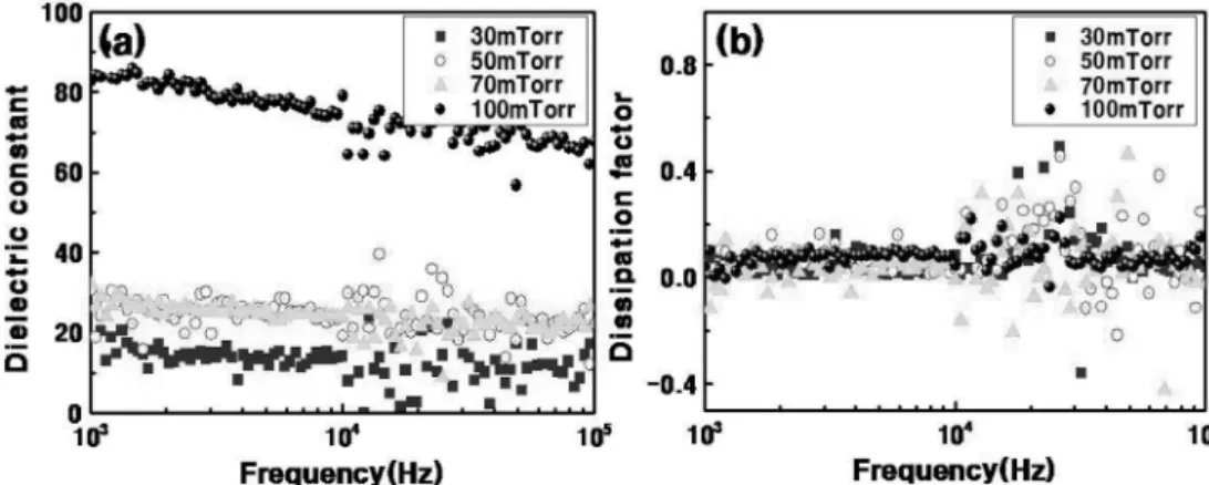
Fig. 6(a) and (b) show the change in dielectric constant and dissipation factor(tan δ) as a function of frequency for BaTiO
3films deposited at various sputtering pressures.
The dielectric constant of the films increased with in- creasing sputtering pressure. The films deposited at 30 to 70 mTorr showed a dielectric constant of 20~30 at 1 kHz.
This is in agreement with those reported for amorphous films.
12,16)On the other hand, the dielectric constant of the films deposited at 100 mTorr showed abnormally high value of ~80 at 1 kHz. The effects of the sputtering pressure on the dissipation factor were negligible. The films showed a dissipation factor of 0.03~0.36 at 1 kHz.
In general, the microstructure of the BaTiO
3films affects the dielectric constant and dissipation factor. In parti- cular, the capacitance of the films increases with increas- ing grain size.
25)From the AFM image in Fig. 4, it can be inferred that the high dielectric constant of the film deposited at 100 mTorr is due to the large crystallite size.
Even though XRD peaks revealed that BaTiO
3films were amorphous states, the variation of dielectric constant could be attributed to size effects of nano-crystallites.
The dielectric constant of the films deposited at 100
Fig. 5. XPS spectra of (a) wide surface scan, (b) Ba3d, (c) Ti2p and (d) O1s obtained from BaTiO
3film.
mTorr was 2~3 times higher than that of the amorphous BaTiO
3films prepared using other methods
12,16)and is 30~40 times higher than those of polymer dielectrics, such as PET and PP.
The leakage current in a high energy density capacitor should be as low as possible to optimize the storage capacity. Fig. 7(a) shows the leakage current character- istics of the BaTiO
3films. The leakage current increased gradually with increasing sputtering pressure. The leakage current was reported to be affected by the grain size, crystallinity and surface morphology.
26)The increase in leakage current of the film with sputtering pressure was attributed to the increase in surface roughness. The film deposited at 50 mTorr showed fluctuations of the leakage current due to self healing, which is the ability to recover after instantaneous breakdown. The leakage current of the BaTiO
3films was approximately 10
−11~ 10
−8A at 400 kV/cm. The polarization-electric field(P-E) properties of the BaTiO
3films were measured up to ~100 kV/cm (Fig.
7(b)). The films deposited at 30~70 mTorr showed almost linear responses, suggesting a field independent dielectric constant. On the other hand, the film at 100 mTorr ex- hibited a loop shaped curve. As indicated in Fig. 6(a), the films deposited at 30~70 mTorr showed low polarization values due to the low dielectric constant, and the film deposited at 100 mTorr showed a higher polarization
value. The BaTiO
3film at 100 mTorr showed polarization of 8 µC/cm
2at 100 kV/cm and remnant polarization(P
r) of 2 µC/cm
2.
4. Conclusion
This study examined the effects of the sputtering pres- sure during sputtering on the microstructure, surface morphology, deposition rate and electrical properties of sputter deposited BaTiO
3films. The sputtering pressure is the key deposition parameter affecting the electrical properties and stable preparation of BaTiO
3films.
Although they were prepared at room temperature, high quality BaTiO
3films with a high dielectric constant and low leakage current could be obtained by controlling the sputtering pressure during sputtering. The BaTiO
3films prepared at 100 mTorr showed a dielectric constant of
~80 at 1 kHz and a leakage current of 10
−8A at 400 kV/
cm. This suggests that flexible BaTiO
3films prepared by sputtering are promising dielectrics for high energy density capacitors.
Acknowledgements
This study was supported by Basic Science Research Program through the National Research Foundation of Fig. 6. (a) Dielectric constant and (b) dissipation factor of the BaTiO
3films deposited at a range of pressures.
Fig. 7. (a) Current-voltage plots and (b) polarization-electric field curves of BaTiO
3films deposited at a range of pressures.
Korea(NRF) funded by the Ministry of Education, Science and Technology(No. 2012-0004538) and by a Kyungpook National University Research Fund, 2012.
References
1. M. T. Domonkos, S. Heidger, D. Brown, J. V. Parker, C.
W. Gregg, K. Slenes, W. Hackenberger, S. Kwon, E.
Loree and T. Tran, IEEE Trans. Plasma Sci., 38, 2686 (2010).
2. W. J. Sarjeant, J. Zirnheld and F. W. MacDougall, IEEE Trans. Plasma Sci., 26, 1368 (1998).
3. L. Hua, L. Fuchang, Z. Heqing, D. Ling, H. Yongxia and K. Zhonghua, IEEE Trans. Magn., 45, 327 (2009).
4. J. L. Nash, Polymer Eng. Sci., 28, 862 (1988).
5. N. Zebouchi and D. Malec, J. Appl. Phys., 83, 6190 (1998).
6. P. Karanja and R. Nath, IEEE Trans. Electr. Insul., 28, 294 (1993).
7. G. Love, J. Am. Ceram. Soc., 73, 339 (1990).
8. G. Brennecka, J. Ihlefeld, J-P. Maria, B. Tuttle and P.
Clem, J. Am. Ceram. Soc., 93, 3935 (2010).
9. J. Kim, D. Kim, J. Kim, Y. Kim, K. N. Hui and H. Lee, Electron. Mater. Lett., 7, 155 (2011).
10. J. Lim, S. Zhang and T. R. Shrout, Electron. Mater. Lett., 7, 71 (2011).
11. G. H. Jain, L. A. Patil, M. S. Wagh, D. R. Patil, S. A.
Patil and D. P. Amalnerkar, Sens. Actuators, B117, 159 (2006).
12. F. El. Kamel, P. Gonon, F. Jomni and B. Yangui, J. Eur.
Ceram. Soc., 27, 3807 (2007).
13. J. Zeng, H. Wang, M. Wang, S. Shang, Z. Wang and C.
Lin, Thin Solid Films, 322, 104 (1998).
14. D. Kim, S. Lee, Y. Park and S. Park, Mater. Lett., 40, 146 (1999).
15. B. Lee and J. Zhang, Thin Solid Films, 388, 107 (2001).
16. C. H. Wu, J. P. Chu, S. F. Wang, T. N. Lin, W. Z. Chang and V. S. John, Surf. Coat. Technol., 202, 5448 (2008).
17. Q. X. Jia, Z. Q. Shi and W. A. Anderson, Thin Solid Films, 209, 230 (1992).
18. T. Minami, S. Ida and T. Miyata, Thin Solid Films, 416, 93 (2002).
19. V. Assuncao, E. Fortunato, A. Marques, H. Aguas, I.
Ferreira, M.E.V. Costa and R. Martins, Thin Solid Films, 427, 402 (2003).
20. P. K. Song, Y. Irie, S. Ohno, Y. Sato and Y. Shigesato, Jpn. J. Appl. Phys., 43, 442 (2004).
21. P. Zeman and S. Takabayashi, Surf. Coat. Technol., 153, 93 (2002).
22. L. I. Maissel and R. Glang, Handbook of Thin Film Technology, p.22, Mcgraw-Hill Inc, New York, USA, (1970).
23. S. M. Mukhopadhyay and T. C. S Chen, J. Mater. Res., 10, 1502 (1995).
24. S. A. Nasser, Appl. Surf. Sci., 157, 14 (2000).
25. H. Kawano, K. Morii and Y. Nakayama, Mater. Lett., 12, 252 (1991).
26. Y. B Chen, C. L. Huang, Surf. Coat. Technol., 201, 643 (2006).