Korean J. Mater. Res.
Vol. 29, No. 10 (2019)
586
Doping Effect of Yb
2O
3on Varistor Properties of ZnO-V
2O
5-MnO
2-Nb
2O
5Ceramic Semiconductors
Choon-Woo Nahm †
Department of Electrical Engineering, Dongeui University, Busan 47340, Republic of Korea (Received July 24, 2019 : Revised September 9, 2019 : Accepted September 11, 2019)
Abstract
This study describes the doping effect of Yb2
O3
on microstructure, electrical and dielectric properties of ZnO-V2
O5
- MnO2
-Nb2
O5
(ZVMN) ceramic semiconductors sintered at a temperature as low as 900°C. As the doping content of Yb2
O3
increases, the ceramic density slightly increases from 5.50 to 5.54 g/cm3
; also, the average ZnO grain size is in the range of 5.3-5.6 μm. The switching voltage increases from 4,874 to 5,494 V/cm when the doping content of Yb2
O3
is less than 0.1 mol%, whereas further doping decreases this value. The ZVMN ceramic semiconductors doped with 0.1 mol% Yb2
O3
reveal an excellent nonohmic coefficient as high as 70. The donor density of ZnO gain increases in the range of 2.46-7.41×10¹⁷
cm−3
with increasing doping content of Yb2
O3
and the potential barrier height and surface state density at the grain boundaries exhibits a maximum value (1.25 eV) at 0.1 mol%. The dielectric constant (at 1 kHz) decreases from 592.7 to 501.4 until the doping content of Yb2
O3
reaches 0.1 mol%, whereas further doping increases it. The value of tanδ increases from 0.209 to 0.268 with the doping content of Yb2
O3
.Key words
Yb2
O3
, doping effect, microstructure, electrical properties, varistors.1. Introduction
Varistor is resistor in which the resistance varies with voltage in a nonohmic relation. 1,2) Varistor has high resistance and is excellent resistor, if any voltage is below critical voltage. When the applied voltage exceeds critical voltage, the resistance of the varistor suddenly decreases and the electrical current abruptly increases.
Basically, due to these varistor properties, the varistor possesses the ability to absorb various surges and prevent electrical appliances, electronic passive and active components from being damaged by surges. 3)
Ceramic varistor is fabricated from metal oxide powder with high purity. Among a lot of materials, the main varistor type is zinc oxide (ZnO), which is nonstoichiometric n-type semiconductor having excess Zn. To change ZnO of low conductivity to ceramic semiconductors of much higher conductivity, the oxides such as bismuth, cobalt, manganese and others should be added to ZnO by small content. Based on usage of varistor, firstly diverse additives are designed to obtain satisfactory solution.
The microstructure structure of ZnO varistor consists
of numerous semiconducting grains separated by grain boundaries. As it were, this is like to the microstructure of a polycrystalline. One grain boundary between grain and grain is like to one pn junction. 2-,4) As a result, varistors possess three dimensionally a lot of pn junctions, that is, multi-junction. If the junction is not active, the potential barrier will be not generated and then the ohmicity will appear. However there is no how confirm it. Most of varistor are assumed to be active. Owing to multi-junction, the varistor can block or pass the current according to the applied voltage condition. 3,4)
Today, commercial multilayered varistors are largely classified into three: bismuth-based, praseodymium-based, and borosilicate-lead-zinc glass-based. These are obtained by sintering at a temperature above 1,000 o C. 1,5,6) Therefore, the internal electrode within varistors should be expensive palladium (Pd) or platinum (Pt). By the way, adding V 2 O 5 to ZnO varistors may allow ceramic semiconductors to sinter at low temperatures. That is, ZnO-V 2 O 5 -based ceramic semiconductors can be sintered at below 900 o C.
This is a big advantage because ZnO-V 2 O 5 -based ceramic semiconductors can be cofired with silver (Ag) inner-
† Corresponding author
E-Mail : [email protected] (C.-W. Nahm, Dongeui Univ.)
© Materials Research Society of Korea, All rights reserved.
This is an Open-Access article distributed under the terms of the Creative Commons Attribution Non-Commercial License (http://creative-
commons.org/licenses/by-nc/3.0) which permits unrestricted non-commercial use, distribution, and reproduction in any medium, provided the
original work is properly cited.
electrode instead of the expensive Pd or Pt. 7,8) However, currently, the ZnO-V 2 O 5 -based ceramic semiconductors are not being applied to field due to characteristics, reliability and so on. 9-12) Therefore, it is necessary to be continuously researched in diverse aspects such as dopants and sintering conditions for applications. 13-19)
In this work, the doping effect of Yb 2 O 3 on microstructure, E-J and C-V, and dielectric properties of ZnO-V 2 O 5 - MnO 2 -Nb 2 O 5 varistors were examined. Furthermore, the mutual correlation between diverse characteristic parameters was analyzed. And the important one of this research is to report the fact that Yb 2 O 3 -doped ZnO-V 2 O 5 -MnO 2 - Nb 2 O 5 varistors revealed excellent nonohmic properties ( α = 70).
2. Experimental procedure 2.1 Specimen preparation
Metal oxide powder of high purity (> 99.9 %) for varistors were prepared with the following composition ration: (97.4-x) % ZnO, 0.5 % V 2 O 5 , 2.0 % MnO 2 , 0.1 % Nb 2 O 5 , x % Yb 2 O 3 (x = 0.0, 0.05, 0.1, and 0.25 mol).
The powder composition was obtained by conventional blending using ZrO 2 balls ( ϕ 10 mm) and acetone in pp- bottle of 250 ml (Nalgene) for 24 h. The blended powder was dried, mixed with polyvinyl butyral binder, and pressed into pellets of disk shape ( ϕ 10 mm × t 1.5 mm) at a pressure of 100 MPa. The disk-pellets were sintered at 900 o C in air for 3h and thereafter cooled at 4 o C/min.
The disk-pellets were lapped and polished in exact dimension ( ϕ 8 mm × t 1.0 mm). A silver paste was painted on both pellet sides through screen printer and thereafter heated at 550°C for 10 min.
2.2 Microstructure analysis
The samples for microstructure were lapped and polished using a SiC paper and Al 2 O 3 powder and then chemically etched using an HClO 4 –H 2 O solution. The surface was analyzed in a field emission scanning electron microscope (FE-SEM Model Quanta 200, Czech). The average grain size (d) was determined by the lineal intercept method. 20) The ceramic phases generated were analyzed by an X- ray diffraction (XRD Model X¢pert-PRO MPD, the Netherlands) using CuK α radiation. The ceramic density (ρ) was measured using a density determination kit (238490).
2.3 Electrical and dielectric measurement
The V-I measurements of the samples were performed using a high voltage source measure unit (Model Keithley 237, USA). The switching voltage (V 1 mA ) was estimated at a current density of 1.0 mA/cm 2 and the density of leakage current (J L ) was estimated at 0.80 V 1 mA . Furthermore, the
nonohmic coefficient (a) was estimated from the following expression, α = 1/(logV 2 – logV 1 ), where V 1 and V 2 are the switching voltage corresponding to 1.0 mA/cm 2 and 10 mA/cm 2 , respectively.
The C-V measurements of the samples were carried out using an LCR meter (Model QuadTech 7600, USA) and an electrometer (Model Keithley 617, USA). The donor density (N d ), potential barrier height (Φ b ), surface state density (N s ) were determined from the expression proposed by M. Mukae et al.. 21)
The f-C APP ' relation and dissipation factor (tanδ) were performed by using an LCR meter (Model QuadTech 7600, USA).
3. Results and Discussion
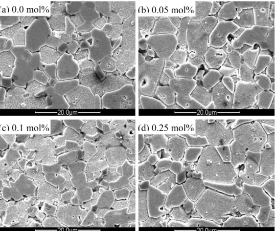
The SEM images of the samples with various doping contents of Yb 2 O 3 are indicated in Fig. 1 The images show typical varistor microstructure regardless of the doping content of Yb 2 O 3 . The variation trend of the average ZnO grain size and the ceramic density of the samples according to the doping content of Yb 2 O 3 are indicated in Fig. 2. The average ZnO grain size decreased from 5.5 to 5.3 μm until the doping content ofYb 2 O 3 reaches 0.1 mol%, whereas a further doping has reversely increased up to 5.6 μm at 0.25 mol% Yb 2 O 3 . The YbVO 4 phase (see Fig. 3 in advance) is like to restrict the grain growth, whereas too much YbVO 4 phase has rather enhanced the grain growth. On the other hand, the ceramic densities (r) slightly increased from 5.50 to 5.54 g/cm 3 . The reason why the additive Yb 2 O 3 increases the ceramic density is like to be attributed to the increase of the content of YbVO 4 with the doping content of Yb 2 O 3 .
The XRD profiles of the samples for various doping contents of Yb 2 O 3 are indicated in Fig. 3. The XRD patterns show the minor phases such as Zn 3 (VO 4 ) 2 , ZnV 2 O 4 , and VO 2 generated in all the samples, with ZnO grains as a major phase. In addition, the samples doped with Yb 2 O 3
revealed YbVO 4 as a secondary phase by showing the diffraction peak at a diffraction angle θ = 25.39 and 33.93.
The peak of YbVO 4 gradually increased with increasing the doping content of Yb 2 O 3 . The YbVO 4 phase may significantly affect V-I properties as shown in Table 1.
The estimated microstructure characteristic parameters are indicated in Table 1.
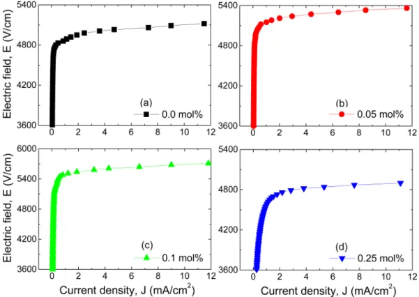
The modified V-I characteristics (E-J) of the samples for various doping contents of Yb 2 O 3 are indicated in Fig. 4.
The varistors have the ability to block or pass currents
through its nonohmicity or ohmicity. Current-blocking is
done at prebreakdown region and current-passing is done
at breakdown region. As can be seen through curve shapes
in Fig. 4, the doping of Yb 2 O 3 significantly affects the
nonohmic properties of varistors. The switching voltage
(V 1 mA ) increased from 4,874 to 5,494 V/cm when the doping content of Yb 2 O 3 is less than 0.1 mol%, whereas a further doping has rather decreased V 1 mA -value up to 4,574 V/cm at 0.25 mol% Yb 2 O 3 . The variation trend of V 1 mA -value depends on firstly grain size and secondly switching voltage (v gb ) of a single grain boundary. As a result, the V 1 mA -value will be more affected by
microstructure.
The variation trend of the nonohmic coefficient and the the density of leakage current of the samples with according to the doping content of Yb 2 O 3 are indicated in Fig. 5. The nonohmicity in the E-J characteristic curves is characterized by the nonohmic coefficient (α). The α-value markedly Fig. 1. SEM images of the samples with various doping contents of Yb 2 O 3 .
Fig. 2 Average grain size and sintered density of the samples with
various doping contents of Yb 2 O 3 . Fig. 3. XRD patterns of the samples with various doping contents
of Yb 2 O 3 : (a) 0.0 mol%, (b) 0.05 mol%, (c) 0.1 mol%, and (d) 0.25
mol%.
increased from 51 to 70 until the doping content of Yb 2 O 3
reaches 0.1mol%, whereas a further doping has abruptly decreased α-value up to 34.4 at 0.25 mol% Yb 2 O 3 . The results show that the doping of Yb 2 O 3 had an obvious effect on the nonohmic properties. The varistors doped with 0.1 mol% Yb 2 O 3 revealed the highest α-value (70), compared with existing ZnO-V 2 O 5 -based varistors. 18,19) The key point of this paper is that an excellent nonohmicty can be obtained from ZVMN-Yb 2 O 3 varistors. The reason why the varistor doped with 0.25 mol% Yb 2 O 3 exhibited lower α-value than that of Yb 2 O 3 -free is assumed to be the result of the excess YbVO 4 phase as mentioned in XRD analysis. This excess YbVO 4 phase may have a significant effect on the potential barrier height at the grain boundaries. As a result, that will decrease the potential barrier height (see Table 2 in advance) and then it is
Fig. 4. E-J characteristics of the samples with various doping contents of Yb 2 O 3 .
Fig. 5. Nonlinear coefficient and leakage current density of the samples with various doping contents of Yb 2 O 3 .
Table 2. C-V and dielectric characteristic parameters of the samples with various doping contents of Yb 2 O 3 .
Yb 2 O 3 content (mol%)
N d (10 17 cm − 3 )
Φ b (eV)
N s (10 12 cm − 2 )
ε APP ' (1 kHz)
tan δ (1 kHz)
0.0 2.46 1.01 1.53 592.7 0.209
0.05 4.09 1.09 2.05 536.0 0.210
0.1 5.75 1.25 2.60 501.4 0.221
0.25 7.41 0.76 2.30 715.9 0.268
Table 1. Microstructure and J-E characteristic parameters of the samples with various doping contents of Yb 2 O 3 .
Yb 2 O 3 content (mol%)
d (μm)
ρ (g/cm 3 )
V 1 mA (V/cm)
v gb
(V/gb) α J L
(μA/cm 2 )
0.0 5.5 5.50 4874 2.7 51.0 56.8
0.05 5.4 5.51 5145 2.8 61.3 60.6
0.1 5.3 5.52 5494 2.9 70.0 84.1
0.25 5.6 5.54 4574 2.6 34.4 262.2
concluded that the α-value abruptly decrease. Meanwhile, as the doping content of Yb 2 O 3 increases, the density of leakage current (J L ) increased from 56.8 to 262.2 μA/
cm 2 . On the whole, although the nonohmic coefficient is high, the leakage current of the samples is high. The leakage current is related to prebreakdown region, of three regions: prebreakdown region (ohmicity), breakdown region (nonohmicity), and upturn region (ohmicity). A high leakage current in prebreakdown region is attributed to the recombination between holes and electrons at the grain boundaries. Furthermore, J L -value is not unrelated to the electron density (see Table 2 in advance). The estimated E-J characteristic parameters are indicated in Table 1.
The C-V characteristics of the samples for various doping contents of Yb 2 O 3 are indicate in Fig. 6. The C-V characteristic parameters, such as donor density (N d ), potential barrier height (Φ b ), and surface state density at the interfaces of grain boundaries (N s ), are indicated in Table 2. The N d -value significantly increased in the range of 2.46-7.41 × 10 17 cm −3 , as the doping content of Yb 2 O 3
increases.
The increase of donor density due to doping content of Yb 2 O 3 is like to be ascribed to the generation of electron according to partially substitution between Yb and Zn, on the basis of following chemical-defect reaction expression:
. Therefore, Yb is obviously donor. The potential barrier height (Φ b ) formed at the grain boundaries increased from 1.01 to 1.25 eV until the doping content of Yb 2 O 3 reaches 0.1 mol%, whereas a further doping has rather decreased Φ b -value up to 0.76 eV at 0.25 mol% Yb 2 O 3 . The variation trend of N s -value with the doping content of Yb 2 O 3 is similar to that of Φ b -value. The a, Φ b , and N s exhibited the same variation trend. As a result, E-J and C-V characteristics are electrically well correlated.
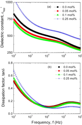
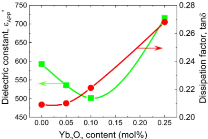
The dielectric properties of the samples with various doping contents of Yb 2 O 3 are indicated in Fig. 7. On the whole, the dielectric constant ε APP ' decreased with increasing frequency, whereas not monotonously. This behavior is directly related to the rotation of the electric dipole, which induces the interfacial polarization and the oriental polarization with frequency. The variation trend of the dielectric constant ε APP ' (at 1 kHz) with the doping content of Yb 2 O 3 is indicated in Fig. 8. The dielectric constant ε APP ' (at 1 kHz) decreased from 592.7 to 501.4 until the doping content of Yb 2 O 3 reaches 0.1 mol%, whereas a further doping has rather decreased ε APP ' up to 715.9 at 0.25 mol% Yb 2 O 3 . The behavior of dielectric constant ε APP ' with the doping content of Yb 2 O 3 completely agreed to the behavior of the average ZnO grain size in microstructure, however it showed the opposite trends to the switching voltage in E-J characteristics. As a result, the dielectric properties are obviously affected by microstructure.
Meanwhile, the dissipation factor (tanδ) exhibited similar and unique curves for all samples with increasing frequency.
In other words, all the samples exhibited valley-point and peak-point with increasing frequency. In general, it can frequently observe this phenomenon in varistors. The
2e' O 2 1 O 2 2Yb O
Yb
2 3
⎯ZnO
⎯ →⎯ •Zn
+O
+ /2
+Fig. 6. C-V characteristics of the samples with various doping contents of Yb 2 O 3 .
Fig. 7. Dielectric characteristics of the samples with various doping
contents of Yb 2 O 3 .
valley-point shows a minimum dielectric loss, and then ε APP '-value is constant. However, peak-point, that is, absorption peak exhibit a loss peak, and then ε APP '-value shows an abrupt decrease. The behavior of the dissipation factor tanδ (at 1 kHz) with the doping content of Yb 2 O 3 is indicated in Fig. 8. The tanδ-value increased from 0.209 to 0.268 with the doping content of Yb 2 O 3 . The variation trend of tanδ-value with the doping content of Yb 2 O 3 is similar to those of J L -value and N d -value. In light of the variation trend of tanδ, J L , and N d , it is obvious that J L - value is affected by N d -value, and tanδ is affected by J L - value. Where, on the basis of the related data, the ZVMN-Yb 2 O 3 varistors show that their characteristics are electrically and dielectrically well correlated. A few dielectric parameters with doping content of Yb 2 O 3 are indicated in Table 2.
4. Conclusions
The doping effect of Yb 2 O 3 on microstructure and electrical properties of ZnO-V 2 O 5 -MnO 2 -Nb 2 O 5 (ZVMN) varistors was examined. The change of 0-0.25 mol% in the doping content of Yb 2 O 3 has a meaningful effect on varistor properties, in particular, nonohmic coefficient, unlike microstructure. The doping effect of Yb 2 O 3 is not large in microstructure, whereas the slight variation of microstructure has a significant effect on electrical and dielectric properties. The average ZnO grain size and switching voltage is not fully decreased or fully increased in full range (0-0.25 mol%) the doping content of Yb 2 O 3 . However, the variation trend between them was the same. The nonohmic coefficient (α) as the core parameter of varistor exhibited a maximum value (α = 70) when the doping content of Yb 2 O 3 is 0.1 mol%. Then potential
barrier height (Φ b ) and surface state density (N s ) also exhibited maximum value. The a, Φ b , and N s exhibited the same variation trend. As a result, it is verified that E- J and C-V characteristics are electrically well correlated.
The electron density (N d ) increased with the doping content of Yb 2 O 3 . In the light of this result, Yb obviously serves as a donor. The increase of leakage current with the doping content of Yb 2 O 3 is assumed to be ascribed to the increasing electron density. As a result, the increase of leakage current resulted in the increase of dissipation factor (tand). The variation trend of dielectric constant is correlated to average ZnO grain size. Through this study, it was logically analyzed that the microstructure, electrical and dielectric properties are mutually related. Conclusively, the Yb 2 O 3 -doped ZnO-V 2 O 5 -MnO 2 -Nb 2 O 5 varistors is believed to have sufficient potential as a promising multilayered chip varistors.
References
1. M. Matsuoka, Jpn. J. Appl. Phys., 10, 736 (1971).
2. L. M. Levinson and H. R. Philipp, Am. Ceram. Soc. Bull., 65, 639 (1986).
3. T. K. Gupta, J. Am. Ceram. Soc., 73, 1817 (1990).
4. H. R. Pilipp and L. M. Levinson, J. Appl. Phys., 46, 1332 (1976).
5. K. Mukae, Am. Ceram. Bull., 66, 1329 (1987).
6. C.-W. Nahm and C.-H. Park, J. Mater. Sci., 35, 3037 (2000).
7. J.-K. Tsai and T.-B. Wu, J. Appl. Phys., 76, 481 (1994).
8. J.-K. Tsai and T.-B. Wu, Mater. Lett., 26, 199 (1996).
9. C.-W. Nahm, J. Am. Ceram. Soc., 94, 2269 (2011).
10. C.-W. Nahm, J. Mater. Sci.: Mater. Electron., 22, 444 (2011).
11. C.-W. Nahm, Microelectron. Reliability, 54, 2836 (2014).
12. C.-W. Nahm, J. Mater. Sci.: Mater. Electron., 23,457 (2012).
13. C.-S. Chen, J. Mater. Sci., 38, 1033 (2003).
14. H. Pfeiffer and K. M. Knowles, J. Eur. Ceram. Soc., 24, 1199 (2004).
15. M. Zhao, X. C. Liu, W. M. Wang, F. Gao and C. S. Tian, Ceram. Int., 34, 1425 (2008).
16. Z. Ming, S. Yu and T. C. Sheng, J. Eur. Ceram. Soc., 31, 2331 (2011).
17. M. Mirzayi and M. H. Hekmatshoar, Phys. B (Amsterdam, Neth.), 414, 50 (2013).
18. C.-W. Nahm, J. Alloys Compd., 578, 132 (2013) 19. C.-W. Nahm, J. Korean Ceram. Soc., 55, 504 (2018) 20. J. C. Wurst and J. A. Nelson, J. Am. Ceram. Soc., 55,109
(1972).
21. M. Mukae, K. Tsuda and I. Nagasawa, J. Appl. Phys., 50, 447 (1979).