A Single-Bit 2nd-Order CIFF Delta-Sigma Modulator for Precision Measurement of Battery Current
Gi-Gyeong Bae*, Ji-Min Cheon**
배터리 전류의 정밀 측정을 위한 단일 비트 2차 CIFF 구조 델타 시그마 모듈레이터
배기경*, 천지민**
Abstract In this paper, a single-bit 2nd-order delta-sigma modulator with the architecture of cascaded-of-integrator feedforward (CIFF) is proposed for precision measurement of current flowing through a secondary cell battery in a battery management system (BMS). The proposed modulator implements two switched capacitor integrators and a single-bit comparator with peripheral circuits such as a non-overlapping clock generator and a bias circuit. The proposed structure is designed to be applied to low-side current sensing method with low common mode input voltage. Using the low-side current measurement method has the advantage of reducing the burden on the circuit design. In addition, the ±30mV input voltage is resolved by the ADC with 15-bit resolution, eliminating the need for an additional programmable gain amplifier (PGA). The proposed a single-bit 2nd-order delta-sigma modulator has been implemented in a 350-nm CMOS process. It achieves 95.46-dB signal-to-noise-and-distortion ratio (SNDR), 96.01-dB spurious-free dynamic range (SFDR), and 15.56-bit effective-number-of-bits (ENOB) with an oversampling ratio (OSR) of 400 for 5-kHz bandwidth. The area and power consumption of the delta-sigma modulator are 670⨯490 μm2 and 414 μW, respectively.
요약 본 논문에서는 배터리 관리 시스템 (BMS)에서 2차 전지 배터리를 통해 흐르는 전류의 정밀한 측정을 위한 cascaded-of-integrator feedforward (CIFF) 구조의 단일 비트 2차 델타-시그마 모듈레이터를 제안하였다. 제안된 모듈 레이터는 2개의 스위치드 커패시터 적분기, 단일 비트 비교기, 비중첩 클록 발생기 및 바이어스와 같은 주변 회로로 구현하 였다. 제안된 구조는 낮은 공통 모드 입력 전압을 가지는 low-side 전류 측정 방법에 적용되도록 설계되었다. Low-side 전 류 측정 방법을 사용하면 회로 설계에 부담이 줄어들게 되는 장점을 가진다. 그리고 ±30mV 입력 전압을 15비트 해상도를 가지는 ADC로 분해하기 때문에 추가적인 programmable gain amplifier (PGA)를 구현할 필요가 없어 수 mW의 전력 소모를 줄일 수 있다. 제안된 단일 비트 2차 CIFF 델타-시그마 모듈레이터는 350nm CMOS 공정으로 구현하였으며 5kHz 대역폭에 대해 400의 oversampling ratio (OSR)로 95.46dB의 signal-to-noise-and-distortion ratio (SNDR), 96.01dB의 spurious-free dynamic range (SFDR) 및 15.56비트의 effective-number-of-bits (ENOB)을 달성하였 다. 델타 시그마 모듈레이터의 면적 및 전력 소비는 각각 670⨯490μm2 및 414μW이다.
Key Words : Analog-to-digital converter, battery management system, CIFF, current sensing, delta-sigma modulator
This research was supported in part by Korea Institute for Advancement of Technology(KIAT) grant funded by the Korea Governm ent(MOTIE)(N0001883, The Competency Development Program for Industry Specialist) and in part by Basic Science Research Progr am through the National Research Foundation of Korea(NRF) funded by the Ministry of Education, Science and Technology(2015R1 D1A1A01059206). The EDA tool was supported by the IDEC.
* R&D Center, PIXELPLUS
** Corresponding Author : School of Electronic Engineering, Kumoh National Institute of Technology ([email protected])
Received May 02, 2020 Revised May 29, 2020 Accepted May 29, 2020
1. Introduction
With the growing interest in the eco-friendly and new energy industries, the solar energy and electric vehicle-related industries are receiving a lot of attention, and the battery technology, which is responsible for the storage of electric energy, is particularly attracting attention for efficient energy management. In order to conserve a lot of energy in a single charge, a high energy efficiency battery is required, and thus lithium-ion (Li-ion) batteries are widely used.
The Li-ion battery is one of the rechargeable battery that can be charged and discharged. It has high energy density and excellent storage and life characteristics [1, 2].
Li-ion secondary cells, which is also called Li-ion rechargeable batteries, have positive and negative electrodes inside, and are composed of insulators that prevent these electrodes from contacting each other. The battery may explode if two electrodes touch each other due to a defect of the insulator or an overcurrent flows due to overcharging of the battery. Therefore, there is a need for a battery management system (BMS) that can prevent overcurrent by observing the current, voltage, and temperature of the battery so that the rechargeable battery can operate in a safe area [3].
The BMS is used to balance each cell in the battery, to prevent cell damage through optimal battery control, and to extend the life of the battery to maximize battery performance and ensure battery safety. In general, the BMS operation consists of four stages: monitoring, estimation, control and management, and diagnosis. First, the
remaining capacity and deterioration of the battery are estimated by monitoring analog signals such as voltage, temperature, and current of each cell during charging and discharging. The battery is discharged and cooled to control and manage the charge/discharge rate, temperature, and cell balance. When a failure occurs through diagnosis, the battery is blocked and the user is notified of the failure [4]. For efficient battery management, the voltage, temperature, and current of the battery must be measured more precisely, which requires a high performance sensor interface circuit with low noise, high resolution, and high linearity.
In this paper, we consider the design of the sensor interface circuit to measure the current precisely among the parameters such as voltage, temperature, and current to check the battery operation. In general, there are two measurement techniques for measuring current. The first method is to measure current through the magnetic flux generated in a conductor using a Hall sensor, which is a magnetic field sensing element and the second method is to measure the magnitude of the current by acquiring the magnitude of the voltage across a series of shunt resistors [5-8].
Since the Hall sensor is a magnetic measurement system, it can be placed near a conductor through which current flows without having to be inserted directly into the current path, thereby simplifying installation. However, additional circuitry is required for offset and linearity compensation, and the accuracy is limited. Because the shunt resistor-based sensor is inserted into the current path, it can affect the magnitude of the supply voltage applied to the system and require large
resistors for high precision and resolution.
However, improvements in circuit design and fabrication make it possible to amplify small signals with a low-noise programmable gain amplifier (PGA), so that the current can be measured with high precision even with small shunt resistors. In addition, it has better accuracy, linearity, and offset characteristics than the magnetic current sensor.
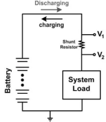
The sensor interface circuit for current measurement used in the BMS must be a low-power and small-area circuit, which requires low noise, high linearity and small offset characteristics for high resolution. In Fig. 1, the PGA is used to amplify the very small voltage generated across the shunt resistor by the current flow and pass it to the analog-to-digital converter (ADC) for high resolution. However, if the ADC is designed to have enough high resolution to detect very small voltages across the shunt resistor, then no PGA circuitry is required and power consumption and chip area can be further reduced.
Fig. 1. Sensor interface circuit for current measurement with a shunt resistor in the BMS
In general, a low-noise ADC with high-resolution is achieved with a delta-sigma ADC architecture. The delta-sigma ADC
effectively suppresses quantization noise with oversampling and noise shaping techniques to achieve high signal to noise ratio (SNR) within the signal band [9]. Therefore, this paper proposes a single-bit 2nd-order delta-sigma modulator to measure battery current with precision for the BMS targeted to a drone application.
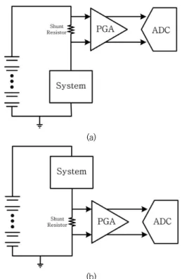
Fig. 2. Current sensing system with a shunt resistor
2. Proposed Single-Bit 2nd-Order
Delta-Sigma Modulator
2.1 Derivation of the Target Specification
In this section, we derive design specifications of the proposed delta-sigma modulator circuit for current measurement of the BMS of secondary cells. The secondary cells are widely used in smartphones, laptops, drones and electric vehicles. Among them, the BMS of battery for the drone, which is rapidly increasing in use, is selected as the targeting application. As a result of investigating the maximum current from the datasheet of the drone battery [10], the discharge rate and capacity of the battery generally used are 15~45 C and 150~1000 mAh, respectively, and the maximum current is 4.58 ~ 25 A as theproduct of the battery capacity and discharge rate. Therefore, since the secondary cell can be charged and discharged, its measurement current range is determined to be ±30 A in consideration of the measurement margin. Fig.
2 shows a block diagram of a shunt resistance-based current measurement system.
The charge and discharge operation can be seen as the relationship between V1 and V2. V2 becomes higher than V1 in the charge operation, and V1 becomes higher than V2 in the discharge operation [11-13].
(a)
(b)
Fig. 3. Current sensing methods with a shunt resistor (a) high-side sensing (b) low-side sensing
In case of measuring current with shunt resistor, it should be connected in series with the circuit, and the method is divided according to where the shunt resistor is located as shown in Fig. 3. The method is divided into a high-side sensing method with a shunt
resistor between the battery and the system and a low-side sensing method with a shunt resistor between the system and ground. The high-side sensing method has the advantage of directly measuring the current flowing through the system with respect to ground, but the high common mode voltage can be a burden on the measurement circuit. On the other hand, the low-side sensing method has a disadvantage in that the ground voltage of the system is the voltage applied to the resistor, but the common mode voltage is near zero, thereby reducing the burden on the circuit design.
Therefore, in this paper, we adopt low-side sensing method that can bring low common mode voltage.
The magnitude of the shunt resistor must be determined by considering the magnitude of the battery voltage and current. If the resistor is too large, the resistor itself consumes a lot of power, and a large voltage is generated across the resistor. On the other hand, if the resistor is too small, there is a very small voltage across it, which places the burden of designing a very large gain for the PGA that amplifies the voltage when the resolution of the ADC is low.
Therefore, in this paper, we aim to resolve the
±30-mV voltage signal by a 15-bit ADC without the PGA using a 1-mΩ shunt resistor with 1-W current-rating. Here, the bandwidth of the voltage signal is considered to be 5 kHz.
2.2 Architecture
In a typical feedback delta-sigma modulator, both the input and output of the integrator are functions of the input, so when a large signal is applied into the input, the amplifier becomes slewing and the signal is distorted by the large output signal of the integrator.
Therefore, allowing only small input signals to avoid this problem increases power consumption because SNR is reduced and amplifiers need to be less noisy. As the output range of the integrator increases, the rate of change in the voltage gain with the signal magnitude increases, resulting in signal distortion. Avoiding this requires a high voltage gain from the amplifier of the integrator.
Under design conditions that require low supply voltage and low consumption power, it is very difficult to design a amplifier to meet both the high voltage gain and wide output range of the amplifier. Therefore, feed forward delta-sigma modulator structures are used instead of feedback delta-sigma modulator structures to address these problems under low power supply conditions [14-16].
To reduce the design burden of the entire circuit of a delta-sigma modulator, a single bit structure is employed, which is simpler than a multi-bit structure. The single-bit structure also has the advantage of reducing the non-ideal characteristics of the fully differential amplifier, capacitors, and switches used in the integrator [17, 18].
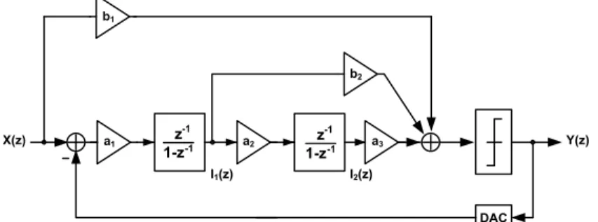
Fig. 4 shows the MATLAB Simulink block diagram for the behavioral simulation of the proposed single-bit 2nd-order delta-sigma
modulator using cascaded of integrator feedfoward (CIFF) structure. When a1=1, a2=1, a3=1, b1=1, and b2=2, the transfer function, which is the relationship between the input and the output, can be expressed as follows.
(1) Note that z is a complex number for z-transform. At the output signal Y, the input signal X comes out without delay, and the quantization noise E is expressed as passing through the 2nd-order high pass filter. In this case, the output signals of the integrators I1and I2 are obtained as follows.
(2)
(3) Equation (2) and equation (3) show that I1 and I2 have nothing to do with the magnitude of X, so if E remains at a low level, the stable output can be produced regardless of the magnitude of X.For the single-bit delta-sigma modulator structure, the output range of the integrator should be reduced to ensure loop filter stability and operate within the supply range [15]. To meet stability and operation voltage range of the integrators, the loop filter’s coefficients are adjusted as a1=1/4, a2=1/3, a3=2/3, b1=1/3, and
Y(z)
X(z)
z
-11-z
-1z
-11-z
-1 b1a1 a2
b2
a3
I1(z) I2(z)
DAC
Fig. 4. MATLAB Simulink Block diagram for the behavioral simulation of the proposed single-bit 2nd-order CIFF
delta-sigma modulator
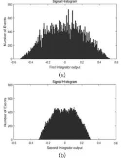
b2=1/2 in the block diagram of Fig. 4. Fig. 5 shows the histograms of the outputs of the first and second integrators, which are obtained by the behavioral simulation. It can be seen that the histograms of the outputs of the first integrator and the second integrator are maintained within about 50% and 30% of the power supply voltage, respectively. These characteristics are maintained even when the input signal is increased by –6 dB relative to the power supply voltage.
(a)
(b)
Fig. 5. Histograms of the outputs of (a) the first integrator and (b) the second integrator
Fig. 6 is the signal to noise and distortion ratio (SNDR) graph obtained by varying the input signal magnitude through MATLAB behavioral simulation. The SNDR rises linearly with the amplitude of the input signal and then decreases rapidly. The maximum allowed input signal amplitude and maximum SNDR for the proposed system are 1.08 V and 103 dB, repectively. Based on this, the input signal amplitude is designed to be 1 V and the reason
for designing with 103-dB SNDR, which is approximately 17-bit effective number of bits (ENOB), is to secure margins due to intrinsic noise and nonlinearity of the circuit itself.
Fig. 6. SNDR graph according to input magnitude of the proposed modulator
In addition, through MATLAB behavioral simulation, the DC gains of the operational transconductance amplifiers (OTAs) used in both the first and the second integrators can be obtained as shown in Table 1. From Table 1, it can be seen that the target SNDR of 103 dB can be achieved when the OTA of the first integrator has a DC gain of more than 60 dB and the OTA of the second integrator has a DC gain of more than 40 dB.
Table 1. SNDR and ENOB according to DC gain of each stage in the proposed modulator
1
st(dB) 2
nd(dB) SNDR (dB) ENOB (bits)
80 80 106.48 17.39
80 60 106.30 17.36
80 40 101.59 16.58
60 80 105.99 17.31
60 60 104.64 17.09
60 40 102.46 16.73
40 80 100.76 16.44
40 60 96.75 15.78
40 40 95.96 15.65
2.3 Circuit Implementation
Fig. 7 shows the proposed single-bit 2nd-order CIFF delta-sigma modulator to achieve high resolution. The proposed delta-sigma modulator circuit is composed of two switched-capacitor integrators, a clock generator, a single bit comparator, and other logic for control and digital signal output.
2.3.1 OTA for 1st-stage integrator
Because the output swing range of the integrator is small owing to the nature of the CIFF architecture, the folded cascode OTA is
adoped to easily achieve DC voltage gain of more than 60 dB while procuring phase margin for stability [18]. The OTA used in the first integrator shown in Fig. 8(a) adopts a fully differential structure to reduce even-order harmonics and increase dynamic range (DR), uses a PMOS input to reduce 1/f noise, and adds the slew-rate compensation circuit to secure the fast settling for large load capacitance. Fig. 8(b) shows a common mode feedback (CMFB) circuit used to stabilize the output common mode of a fully differential OTA.
Fig. 7. Circuit diagram of the proposed single-bit 2nd-order CIFF delta-sigma modulator
(a)
(b)
Fig. 8. OTA for the integrator of 1st-stage (a) PMOS input folded cascode OTA circuit (b) dynamic CMFB circuit
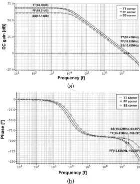
Fig. 9 shows the frequency responses obtained by performing the post-simulations with parasitic effects on the OTA for the first integrator. The simulations are performed under TT corner, FF corner, and SS corner.
Table 2 shows the corner post-simulation results of the OTA. The OTA has 68.78-dB DC gain, 73.80-degree phase margin, and 20.41-MHz unity gain frequency under TT corner.
(a)
(b)
Fig. 9. Frequency response of the OTA for the 1st-stage integrator
Table 2. Corner post-simulation results of the OTA for the 1st-stage integrator
TT FF SS
Power Supply (V) 1.80 1.98 1.62
Temperature (℃) 50 -30 120
Static Current (μA) 70.56 75.90 70.12 DC Voltage Gain (dB) 68.78 68.21 61.18 Phase Margin (°) 73.80 74.10 86.05 Unity Gain Frequency
(MHz) 20.41 18.63 15.02
Slew Rate (V/μs) 29.26 34.43 27.34
Fig. 10. OTA for the integrator of 2nd-stage
(a)
(b)
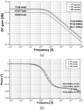
Fig. 11. Frequency response of the OTA for the 2nd-stage integrator
2.3.2 OTA for 2nd-stage integrator
According to the behavioral simulation results in Table 1, it can be seen that the OTA of the second integrator may have a smaller
DC voltage gain than the OTA of the first integrator. In addition, since the load capacitance of the OTA of the second integrator is smaller than that of the OTA of the first integrator, the slew-rate compensation circuit, which is adopted in the OTA of the first integrator, is unnecessary. Therefore, the normal folded cascode OTA of the second integrator is designed as shown in Fig. 10.
Here, the CMFB circuit uses the same circuit used in the OTA in the first stage.
Fig. 11 shows the frequency responses obtained by performing the post-simulations for the second integrator. Table 3 shows the corner post-simulation results of the OTA. The OTA has 53.31-dB DC gain, 86.48-degree phase margin, and 12.34-MHz unity gain frequency under TT corner.
Table 3. Corner post-simulation results of the OTA for the 2nd-stage integrator
TT FF SS
Power Supply (V) 1.80 1.98 1.62
Temperature (℃) 50 -30 120
Static Current (μA) 29.26 30.44 32.64 DC Voltage Gain (dB) 53.31 52.45 52.34 Phase Margin (°) 86.48 86.35 88.06 Unity Gain Frequency
(MHz) 12.34 18.42 11.57
Slew Rate (V/μs) 11.44 12.27 10.57
2.3.3 Single-bit comparator
The characteristics of the single-bit comparator used in the proposed modulator may be relatively less precise, because its nonlinearities are already noise-shaped by the loop filters. Therefore, in place of using the
comparator consisting of the pre-amplifier and offset cancellation circuit of [19], a simple dynamic regenerative comparator is used as shown in Fig. 12.
Fig. 12. Dynamic regenerative comparator
Fig. 13. Circuit diagram of the clock generator for non-overlapping clocks
2.3.4 Non-overlapping clock generator Fig. 13 shows a clock generator for non-overlapping clock generation [20]. The clock generator basically builds a feedback circuit with 2 NAND gates, and a delay circuit, which consists of several inverters, is linked to each NAND output. The inverter gates in the feedback path can be used to adjust non-overlapping intervals and clock delay. The clock generator utilizes the input clock (CLK) to produce clocks P1 and P2. Also, the delayed clocks P1D and P2D are produced from P1 and P2 to carry out the bottom-plate sampling technique that can prevent charge injection from the switches [21].
3. Experimental Results
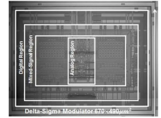
Fig. 14 shows the microphotograph of the fabricated chip. The proposed single-bit 2nd-order CIFF delta-sigma modulator uses 1.8-V supply voltage and is fabricated in 2-poly 4-metal 350-nm CMOS process. A delta-sigma modulator has an area of 670⨯490 μm2 and power consumption of 414 μW. In order to minimize the mismatch caused by the layout, the integrators' OTAs, switches, and capacitors for the implementation of switched capacitor filters are designed symmetrically.
Also, the layout area is divided into an analog circuit area, a mixed signal circuit area, and a digital circuit area to reduce crosstalk noise.
Fig. 14. Microphotograph of the proposed delta-sigma modulator chip
Fig. 15 shows the spectral response of the output of the proposed single-bit 2nd-order CIFF delta-sigma modulator obtained under TT corner with post-simulation on the circuit whose parasitic resistances and capacitances are extracted from the layout result. Table 4 shows the corner post-simulation results of SNDR, Spurious Free Dynamic Range (SFDR), and ENOB for the proposed modulator. When an over-sampling ratio (OSR) of 400 and an input signal of 900 Hz is applied for a 5 kHz
bandwidth, the post-simulation results for TT corner show 95.46-dB SNDR, 96.01-dB SFDR, and 15.56-bit ENOB, while the design target SNDR and ENOB are 103 dB and 17 bits, respectively. This is because there is performance degradation due to the parasitic components and the mismatch between transistors and capacitors by the layout.
Fig. 15. Spectral response of the output signal of the proposed delta-sigma modulator under TT corner with post-simulation
Table 4. Corner post-simulation results
TT FF SS
SNDR (dB) 95.46 95.71 95.29
SFDR (dB) 96.01 95.46 95.92
ENOB (bits) 15.56 15.61 15.53
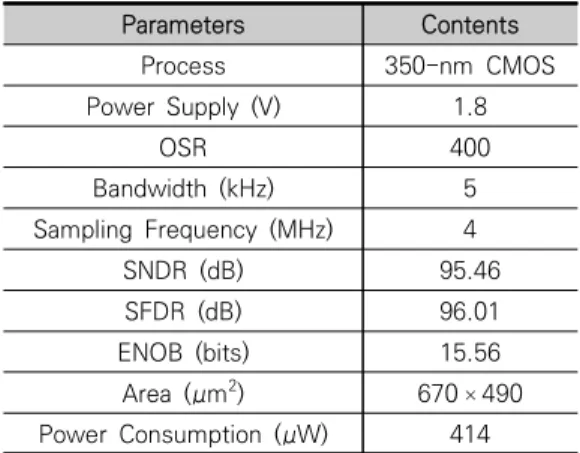
Table 5. Characteristics of the implemented single-bit 2nd-order delta-sigma modulator under TT corner
Parameters Contents
Process 350-nm CMOS
Power Supply (V) 1.8
OSR 400
Bandwidth (kHz) 5
Sampling Frequency (MHz) 4
SNDR (dB) 95.46
SFDR (dB) 96.01
ENOB (bits) 15.56
Area (μm
2) 670⨯490
Power Consumption (μW) 414
Table 5 shows the characteristics of the proposed single-bit 2nd-order CIFF delta-sigma modulator under TT corner.
4. Conclusion
In this paper, we proposed the single-bit 2nd-order delta-sigma modulator with the architecture of CIFF for precision measurement of current flowing through the secondary cell battery in the BMS. The proposed modulator implements two switched capacitor integrators and a single-bit comparator with peripheral circuits such as a non-overlapping clock generator and a bias circuit. The proposed structure is designed to be applied to low-side current sensing method with low common mode input voltage. Using the low-side current measurement method has the advantage of reducing the burden on the circuit design. In addition, the ±30mV input voltage is resolved by the ADC with 15-bit resolution, eliminating the need for the additional PGA. The proposed delta-sigma modulator has been implemented in a 350-nm CMOS process. It achieves
95.46-dB SNDR, 96.01-dB SFDR, and 15.56-bit ENOB with the OSR of 400 for 5-kHz bandwidth. The area and power consumption of the delta-sigma modulator are 670⨯490 μ m2 and 414 μW, respectively.
REFERENCES
[1] L. Lu, X. Han, J. Li, J. Hua, and M.
Ouyang, "A review on the key issues for lithium-ion battery management in electric vehicles", J. Power Sources, vol. 226, pp.
272-288, Mar. 2013.
[2] A. Vayrynen and J. Salminen, "Lithium ion battery production", J. Chem. Thermodyn, vol. 46, pp. 80-85, 2012.
[3] K. W. E. Cheng, B. P. Divakar, H. J. Wu, K.
Ding, and H. F. Ho, "Battery-management system (BMS) and SOC development for electrical vehicles", IEEE Trans. Veh.
Technol., vol. 60, no. 1, pp. 76-88, Jan.
2011.
[4] L. Siguang and Z. Chengning, "Study on battery management system and lithium-ion battery", Proc. Int. Conf. on Computer and Automation Engineering. ICCAE ‘09, pp.
218-222, Mar. 2009.
[5] S. Ziegler, R.C. W, H.H. Iu, L.J. Borle, and J. Borle “Current sensing techniques: A review”, IEEE Sensors Journal, Vol. 9, No. 4, pp. 354-376, 2009.
[6] C. M. Johnson and P. R. Palmer, “Current measurement using compensated coaxial shunts”, Proc. IEE Sci., Measure. Technol., vol. 141, pp. 471-480, Nov. 1994.
[7] J. A. Ferreira, W. A. Cronje, and W. A.
Relihan, “Integration of high frequency current shunts in power electronic circuits”, IEEE Trans. Power Electron., vol. 10, pp.
32-37, 1995.
[8] W. F. Ray and C. R. Hewson, “High performance Rogowski current transducers”, Proc. IEEE Ind. Appl. Conf., pp. 3083-3090, 2000.
[9] S. Pavan, R. Schreier, and G. C. Temes, Understanding Delta-Sigma Data Converters,
NJ, Piscataway:IEEE Press/Wiley, 2017.
[10] https://droneshopperth.com.au/battery-safet y-data-sheets/
[11] F. Cordova and V. Olivares, “Design of Drone Fleet Management Model in A Production System of Customized Products”, Proc. IEEE Int. Conf. on Computers Communications and Control. ICCCC ‘16, pp. 165-172, May 2016.
[12] S.H. Shalmany, D. Draxelmayr, “A ±5 A Integrated Current-Sensing System With
±0.3% Gain Error and 16 μA Offset From -55 ℃ to +85℃”, IEEE J. Solid-State Circuits, vol. 51, no. 4, pp. 800-808, Apr.
2016.
[13] S.H. Shalmany, D. Draxelmayr, “A ±36-A Integrated Current-Sensing System With a 0.3% Gain Error and a 400-μA Offset From -55 ℃ to +85 ℃”, IEEE J. Solid-State Circuits, vol. 52, no.4, pp. 1034-1043, Apr.
2017.
[14] G. Ahn, D. Chang, M. Brown, N. Ozaki, H.
Youra, K. Yamamura, K. Hamashita, K.
Takasuka, G. C. Temes and U. Moon, "A 0.6-V 82-dB delta-sigma audio ADC using switched-RC integrators", IEEE J. Solid-State Circuits, vol. 40, no. 12, pp. 2398-2407, Dec. 2005.
[15] Y. Chae, I. Lee, and G. Han, "A 0.7 V 36 μW 85 dB DR Audio △Σ Modulator Using Class-C Inverter", Proc. IEEE Int. Solid-State Circuits Conf., pp. 490-491, 2008.
[16] J. M. de la Rosa, R. del Río, CMOS Sigma-Delta Converters: Practical Design Guide, NJ, Hoboken:Wiley-IEEE Press, 2013.
[17] J. Roh, S. Byun, Y. Choi, H. Roh, Y.-G.
Kim, and J.-K. Kee, "A 0.9-V 60-μW 1-bit fourth-order delta-sigma modulator with 83-dB dynamic range", IEEE J. Solid-State Circuits, vol. 43, no. 2, pp. 361-370, Feb.
2008.
[18] D. A. Johns and K. Martin, Analog Integrated Circuit Design, New York:Wiley, 1997.
[19] Y. Geerts, M. Steyaert, and W. Sansen,
Design of Multi-Bit Delta-Sigma A/D
Converters, MA, Norwell:Kluwer, 2002.
[20] R. J. Baker, CMOS Mixed-Signal Circuit Design, New York:IEEE Press, 2002.
[21] R. Schreier, J. Silva, J. Steensgaard, and G.
C. Temes, "Design-oriented estimation of thermal noise in switched-capacitor circuits", IEEE Trans. Circuits Syst. I: Reg.
Papers, vol. 52, no. 11, pp. 2358-2368, Nov. 2005.
저자약력
배 기 경 (Gi-Gyeong Bae) [정회원]
⦁2016년 2월 : 금오공과대학교 전 자공학부 (공학사)
⦁2018년 2월 : 금오공과대학교 전 자공학과 (공학석사)
⦁2018년 3월 ~ 현재 :
PIXELPLUS R&D Center 연구원
<관심분야> CMOS Image Sensor, ADC/DAC
천 지 민 (Ji-Min Cheon) [종신회원]