1. Introduction
Recently, Cu
2ZnSnS
4based solar cells has been attracting lot of attention because of its readily available elements, optimum direct band gap of 1.5 eV and high absorption coefficient over 10
4cm
-1makes a promising absorber material for low cost thin film solar cells
1). Solar cells with conversion efficiencies 10%
were achieved with Cu
2ZnSnSSe
4absorbers
2). Since last two decades, many groups have been reported variety of process for growth of CZTS thin films and solar cells
3-14). At present, the most successful method for growing CZTS absorbers is sulfurization of sulfur containing or pure metallic precursors in H
2S or sulfur vapor. The precursors were grown by numerous methods such as evaporation
15), electrochemical
16), sputtering
17), electron beam
18), sol gel
19). To date, highest efficiency is reported on CZTS solar cells is 6.8-7.1% grown by thermal evaporation of precursors followed by a short annealing in sulfur, in this method the precursors were deposited by molecular beam evaporation
15).
Though the evaporation has certain advantages like precise control of composition, it requires above 1,450ºC to evaporate
Cu. A disadvantage of evaporation process is narrow deposition temperature window due to high volatility of sulfide materials.
Evaporation process is also a difficult process to scale up for large area manufacturing. Deposition of metal or alloyed targets by dc magnetron sputtering and selenization of the precursors are one of the most promising processes for production of large area CIGS absorbers
20). Sputtering of precursors and sulfidation for CZTS absorbers have several advantages such as deposition of metal precursors at room temperature in large area with controlled film thickness and controlled composition.
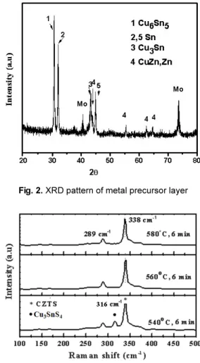
We have grown CZTS absorbers by furnace annealing of Cu/ZnSn/Cu precursors in sulfur ambient at 560ºC for 30 min and achieved 4.6% efficiency in CdS/CZTS solar cells
21). The top Cu layer on precusor acts as a protect layer for the evaporation of tin component. This work is the continuation of the work published in reference 21. Previously, our precursors were annealed in furnace for 30 min. In present work, rapid thermal annealing (RTA) was introduced and the annealing time was shortened to 6 min. We investigated phases and microstructure of CZTS film from the RTF process and applied the film for CZTS solar cells.
Fabrication of Cu 2 ZnSnS 4 Films by Rapid Thermal Annealing of Cu/ZnSn/Cu Precursor Layer and Their Application to Solar Cells
R.B.V. Chalapathy ․ Gwang Sun Jung ․ Young Min Ko ․ Byung Tae Ahn* ․ HyukSang Kwon*
Department of Materials Science and Engineering, Korea Advanced Institute of Science and Technology, 291 Daehak-ro, Yuseong-gu, Daejeon 305-701, South Korea
ABSTRACT: Cu
2ZnSnS
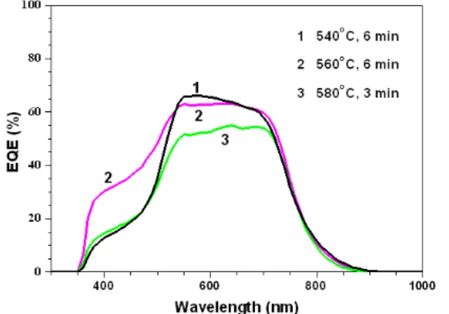
4thin film have been fabricated by rapid thermal annealing of dc-sputtered metal precursor with Cu/ZnSn/Cu stack in sulfur ambient. A CZTS film with a good uniformity was formed at 560ºC in 6 min. Cu
2SnS
3and Cu
3SnS
4secondary phases were present at 540°C and a trace amount of Cu
2SnS
3secondary phase was present at 560ºC. Single-phase large-grained CZTS film with rough surface was formed at 560ºC. Solar cell with best efficiency of 4.7% (V
oc= 632 mV, j
sc= 15.8 mA/cm
2, FF = 47.13%) for an area of 0.44cm
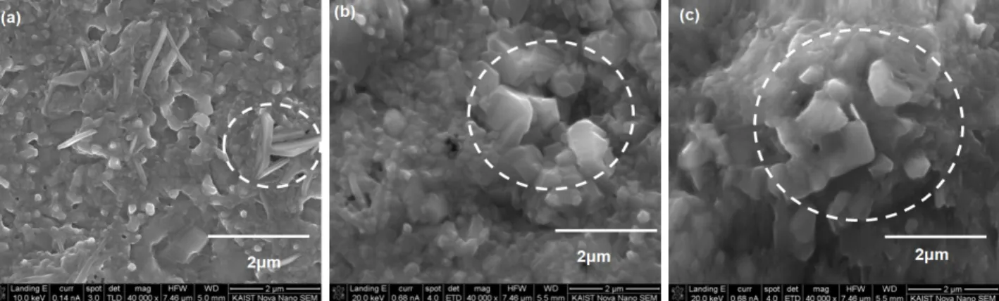
2was obtained for the CZTS absorber grown at 560ºC for 6 min. The existence of second phase at lower-temperature annealing and rough surface at higher-temperature annealing caused the degradation of cell performance. Also poor back contact by void formation deteriorated cell performance. The fill factor was below 0.5; it should be increased by minimizing voids at the CZTS/Mo interface. Our results suggest that CZTS absorbers can be grown by rapid thermal annealing of metallic precursors in sulfur ambient for short process times ranging in minutes.
Key words: Cu
2ZnSnS
4, rapid thermal process, sulfurization, CZTS solar cells
*Corresponding author: [email protected], [email protected] Received November 25, 2013; Revised 2013 29, 2013;
Accepted December 4, 2013
ⓒ 2013 by Korea Photovoltaic Society
This is an Open Access article distributed under the terms of the Creative Commons Attribution Non-Commercial License (http://creativecommons.org/licenses/by-nc/3.0)
which permits unrestricted non-commercial use, distribution, and reproduction in any medium, provided the original work is properly cited.
82