http://dx.doi.org/10.6111/JKCGCT.2014.24.1.041
Passivation properties of SiNx and SiO2 thin films for the application of crystalline Si solar cells
Myung-Il Jeong and Chel-Jong Choi†
School of Semiconductor and Chemical Engineering, Semiconductor Physics Research Center (SPRC), Chonbuk National University, Jeonju 561-756, Korea
(Received January 6, 2014) (Revised February 5, 2014) (Accepted February 7, 2014)
Abstract We have investigated the passivation property of SiNx and SiO2 thin films formed using various process conditions for the application of crystalline Si solar cells. An increase in the thickness of SiNx deposited using plasma enhanced chemical vapor deposition (PECVD) led to the improvement of passivation quality. This could be associated with the passivation of Si dangling bonds by hydrogen atoms which were supplied during PECVD deposition. The SiO2 thin films grown using dry oxidation process exhibited better passivation behavior than those using wet oxidation process, implying the dry oxidation process was more effective in the formation of high quality SiO2 thin films. The relative effective life time gradually decreased with increasing dry oxidation temperature. Such a degradation of passivation behavior could be attributed to the increase in interface trap density caused by thermal damages.
Key words SiNx, SiO2, Passivation, Crystalline Si solar cells, Interface trap density
결정질 실리콘 태양전지 응용을 위한 SiN
x및 SiO
2박막의 패시베이션 특성 연구
정명일, 최철종†
전북대학교 반도체화학공학부, 전주, 561-756 (2014년 1월 6일 접수)
(2014년 2월 5일 심사완료) (2014년 2월 7일 게재확정)
요 약 다양한 공정 조건으로 SiNx와 SiO2 박막을 형성하고 이에 대한 패시베이션 특성에 대한 연구를 수행하였다.
Plasma enhanced chemical vapor deposition(PECVD)을 이용하여 증착된 SiNx 박막의 경우, 증착 두께가 증가함에 따라 페시 베이션 특성이 향상되는 것을 관찰하였다. 이는 PECVD 증착 공정 중 유입되는 수소 원자들이 실리콘 표면에 존재하는
Dangling bond와 결합하여 소수 캐리어의 재결합 현상을 효과적으로 감소시켰기 때문이다. 건식 산화법으로 형성된 SiO2
박막은 습식 산화법으로 형성된 것 보다 치밀한 계면 구조를 가짐으로 인하여 약 20배 이상 우수한 패시베이션 특성을 나 타내었다. 건식 산화 공정 온도가 증가함에 따라 패시베이션 특성이 열화되는 현상이 발생하였고, Capacitance-voltage(C-V) 및 Conductance-voltage(G-V) 분석을 통하여 SiO2/실리콘 계면에 존재하는 계면 결함 밀도 증가에 의해 나타나는 현상임을 알 수 있었다.
1. 서 론
화석연료자원의 유한성으로 인한 고유가 문제와 지구 온난화 방지를 위한 기후변화 협약으로 인하여 신재생에 너지의 개발에 대한 관심과 요구가 크게 증대되고 있다.
특히, 태양전지는 태양광을 전기로 변환시켜주는 반도체 소자로서, 무한 청정 에너지인 태양광이 있는 곳이라면 환경 오염과 소음 발생 없이 반영구적으로 전기를 생산 할 수 있는 환친화적인 신재생 에너지 기술로 전 세계적 으로 각광받고 있다[1-3]. 다양한 종류의 태양전지 가운 데에서 결정질 실리콘 태양전지는 전체 태양광 시장에서 가장 큰 시장을 차지하고 있으며, 고효율화, 저가화 연구 는 계속 되고 있다. 실리콘 태양전지 고효율화를 위한 방법으로는 여러 가지가 있는데 구조적으로 태양전지의
†Corresponding author
†Tel: +82-63-270-3365
†Fax: +82-63-270-3585
†E-mail: [email protected]
전면과 후면으로 나눌 수 있다. 전면에는 표면 조직화와 반사 방지막 증착, 종횡비가 높은 전면전극, 선택적 에미 터 그리고 표면 패시베이션(Surface passivation) 방법이 있고 후면에는 접촉저항이 낮은 후면 전극, 후면 반사 물질 증착, 후면전계(Back surface field) 등이 있다[4].
이 중에 표면 패시베이션 방법은 광전효과로 생성된 소 수 캐리어의 재결합을 줄임으로써 효율을 높이는 방법이 다[5-8]. 다른 고효율화 기술들은 단락전류를 효과적으로 높일 수 있지만, 동시에 개방전압이 낮아지는 상충 되는 면이 있어 태양전지의 효율을 향상시키는데 한계가 있지 만, 표면 패시베이션 방법은 단락전류와 개방전압을 동 시에 높일 수 있기 때문에 태양전지 고효율화에 필수적 인 기술이라 할 수 있다. 지금까지 실리콘 질화막(SiNx), 실리콘 산화막(SiO2), 비정질 실리콘(Amorphous Si), 알 루미늄 산화막(Al2O3), 탄화규소(SiCx) 등 다양한 물질을 사용한 실리콘 태양전지 패시베이션 공정 기술이 제안되 어 지고 있으며, 실리콘 태양전지 효율의 극대화를 위해 더욱더 발전된 고품질 패시베이션 공정 기술에 대한 많 은 연구가 이루어지고 있다[9-12]. 본 연구에서는 다양한 패시베이션 방법 중 P형 실리콘 태양전지에 가장 널리 사용되고 있는 SiNx과 SiO2을 다양한 방법으로 형성하 고 이에 대한 패시베이션의 특성을 연구하였다. 특히, 건 식 산화 온도에 따른 패시베이션 특성 변화 원인을 규명 하기 위해서 Metal-Oxide-Semiconductor(MOS) 소자를 제작하고 계면 결함 밀도(Dit, interface trap density)를 정량적 평가하였다.
2. 실 험
2.1. SDR(Saw damage removal) 및 표면 텍스쳐링 (Surface texturing)
본 연구에서는 붕소(boron)가 도핑된 P형 (100) CZ 단결정 실리콘 기판을 사용하였다. 실리콘 기판의 비저 항과 두께는 각각 0.5~3 cm과 200 µm였다. 먼저 SPM (Surfuric acid peroxide mixture) 용액(H2SO4: H2O2= 1 : 1)과 HPM(Hydrochloric acid and peroxide mixture) 용액(H2O : H2O2: HCl = 6 : 1 : 1)을 이용하여 실리콘 기 판을 세정 한 후 Buffered Oxide Etchant(BOE)를 사용 하여 기판 표면에 존재하는 자연산화막을 제거하였다.
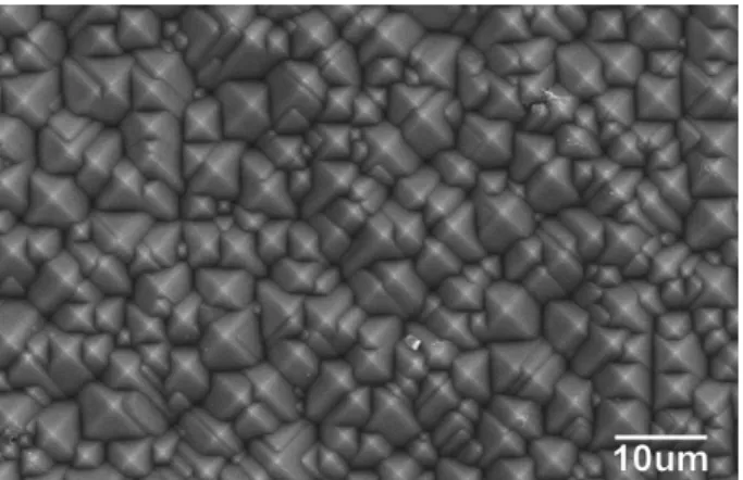
다음으로 45 % KOH 용액을 이용하여 80oC에서 3분 동안 SDR을 진행한 후 초수수로 세정하였다. 마지막으 로 85oC에서 20 wt.% TMAH(Tetramethylammonium hydoroxide)와 IPA(isopropyl alcohol), H2O의 혼합용액 에 30분간 식각하여 실리콘 표면의 텍스처링 공정을 진 행하였다. Fig. 1은 이와 같은 방법으로 표면 텍스쳐링
된 실리콘 기판의 표면 형상을 보여주는 주사전자현미경 결과이다. 비등방석 식각으로 인하여 실리콘 표면에 무 수히 많은 피라미드 형태의 구조가 형성된 것을 관찰 할 수 있다.
2.2. 패시베이션 공정
SDR 및 텍스쳐링 공정을 수행한 후 SiNx 혹은 SiO2
박막을 이용하여 패시베이션 공정을 진행하였다. SiNx
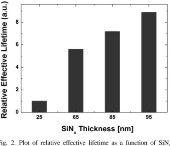
박막은 PECVD(Plasma Enhanced Chemical Vapor Deposition)을 사용하여 SiH4: 25 sccm, NH3: 65 sccm, N2: 70 sccm, 기판 온도: 250oC, 플라즈마 파워 = 0.15 Wcm−2의 조건으로 증착하였다. SiN 증착 두께는 25~95 nm까지 변화 시켰다. SiO2 패시베이션 박막은 다양한 온도에서 Furnace를 이용하여 건식 혹은 습식 산화법으 로 형성하였다. SiO2박막 두께는 산화 방법에 상관없이 모두 100 nm로 동일하게 유지하였다. SiNx및 SiO2박막 의 박막패시베이션 특성을 평가하기 위해서 quasi-steady state photo-conductance(QSSPC)를 이용하여 각각의 공 정 조건별로 유효 소수 캐리어 수명을 분석하였다.
3. 실험결과 및 고찰
Fig. 2는 PECVD로 증착된 SiNx 두께에 따른 패시베 이션 특성을 보여주는 결과이다. SiNx 두께가 증가함에 따라 유효 소수 캐리어 수명이 점진적으로 증가하는 것 을 관찰 할 수 있다. PECVD를 이용하여 SiNx를 증착 할 경우, 수소 가스가 유입되는데, 이러한 수소는 실리콘 표면의 존재하는 실리콘 Dangling bond와 결합하게 된 다. 일반적으로 Dangling bond는 태양광에 여기 되어 전면 전극으로 이동하는 소수 캐리어(P형 태양전지에서 는 전자)의 재결합 장소 역할을 하게 된다. 즉, 수소가 Dangling bond와 결합할 경우, 소수 캐리어의 재결합 Fig. 1. Plan-view SEM image taken from the textured Si surface.
현상을 효과적으로 줄일 수 있다[13]. 따라서 실리콘 질 화막의 두께가 증가될수록 같은 가스 유량과 플라즈마 파워에 PECVD 공정시간은 늘어나기 때문에 수소의 유 입은 더욱더 많아지므로 더 많은 Dangling bond가 수소 와 결합하게 되어 SiNx 두께가 증가할수록 패시베이션 특성이 향상되는 것으로 판단된다[14].
Fig. 3(a)는 습식 혹은 건식 산화법으로 형성된 SiO2의 패시베이션 특성을 비교한 결과이다. 형성된 SiO2 박막 의 두께가 100 nm로 동일함에도 불구하고 건식 산화법 으로 형성된 SiO2 박막이 습식 산화법 SiO2 박막과 비 교하여 약 20배 이상 패시베이션 특성이 우수한 것을 확인 할 수 있다. 이러한 이유는 수증기를 이용한 습식 산화법의 빠른 산화 속도 때문에 건식 산화법으로 형성 한 SiO2의 구조보다 조밀하지 못하게 되고 결과적으로 SiO2 박막과 실리콘 사이의 계면에도 소수 캐리어 재결
합 장소인 결함이나 Dangling 결합이 다량으로 형성되 기 때문이다[15]. 반면 Fig. 3(b)에서 보이는 것처럼, 우 수한 패시베이션 특성을 보이는 건식 산화법으로 형성된
SiO2 박막도 산화 온도에 따라 그 특성이 변화하는 것을
알 수 있다. 즉, 건식 산화 온도가 900oC에서 1000oC로 증가함에 따라 약 16 % 정도 패시베이션 특성이 감소하 는 것을 관찰하였다.
앞서 설명한 것처럼, 실리콘과 패시베이션 박막 사이 의 계면에 존재하는 실리콘 Dangling bond와 같은 계면 결함은 패시베이션 특성을 좌우하는 가장 큰 주요 인자 이다. 따라서, 건식 산화 온도에 따른 패시베이션 특성의 변화는 패시베이션 박막 사이의 계면에 존재하는 계면 결함의 밀도의 관점에서 설명할 수 있다. 건식 산화 온 도 변화에 대한 계면 결함 밀도의 정량적 평가를 위해서 건식 산화법으로 SiO2 박막을 형성하고 100 nm 두께의 백금(Pt) 금속 전극을 상부 및 하부에 형성하여 Fig. 4에 삽입된 그림과 같은 구조로 MOS 소자를 제작한 후 capacitance-voltage(C-V) 및 conductance-voltage(G-V) 분석을 수행하였다. 백금 금속 전극 면적은 300 × 300 µm2이며 Photolithography 공정을 이용하여 패터닝하였 다. MOS 소자에 적용된 SiO2는 800~1000oC에서 5분간 건식 산화법으로 형성하였다. Fig. 4(a)에서 보이는 것처 럼, 건식 산화 온도가 증가함에 따라 Capacitance 값이 점진적으로 감소되는 것을 알 수 있다. 이는 산화 온도 증가에 의해 형성되는 SiO2 박막의 두께가 증가하였기 때문이다. Equivalent Oxide Thickness(EOT)와 Flatband Voltage(VFB)는 양자역학 시뮬레이션을 통하여 계산하였 으며[16], Table 1에서 정리 하였다. 건식 산화 온도가 800oC인 시편의 경우, EOT는 4.5 nm, VFB는 −0.052 V 였지만, 1000oC인 시편의 경우 EOT는 5.0 nm로 약 0.5 nm SiO2두께가 증가하였고, VFB는 0.085 V로 약 0.14 V
Fig. 3. Variation of relative effective lifetime for SiO2 thin film formed using various process conditions.
Fig. 2. Plot of relative effective lifetime as a function of SiNx thickness.
만큼 이동한 것을 알 수 있다. Fig. 4(b)는 동일한 MOS 소자에 대한 G-V 특성 곡선 결과이다. 모든 시편에서 VFB 근처에서 Peak conductance가 관찰되었고, peak의 높이가 건식 산화 온도에 비례하여 증가하는 것을 알 수 있다. 일반적으로 G-V 특성 곡선에서 관찰되는 Peak conductance를 이용하여 계면 결함 밀도(Dit)는 다음과 같은 관계식으로부터 계산할 수 있다[17].
(1)
(2)
Gp: peak conductance, ω: angular frequency q:
electronic charge, Cox: oxide capacitance, Gm: measured conductance, Cm: measured
식(1)과 식(2)를 이용하여 계산된 계면 결함 밀도를 Fig.
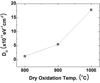
5에 요약 정리하였다. 결함 밀도가 건식 산화 온도에 크 게 의존하는 것을 관찰 할 수 있다. 예를 들어, 건식 산 화 온도가 800oC인 MOS 소자의 경우, 계면 결함 밀도 는 1.23 × 10¹¹eV−1cm−2였지만, 1000oC에서 건식 산화된 MOS 소자에서는 1.78 × 10¹²eV−1cm−2로 약 10배 이상 계면 결함 밀도가 급격하게 증가된 것을 알 수 있다. 즉, 건식 산화 온도의 증가는 계면 밀도 증가를 수반하게 된 다는 것을 알 수 있다. 이러한 현상은 고온에서 건식 산 화 공정 시 공급되는 산소 원자들이 실리콘 원자와 반응이 격렬하게 진행되어 실리콘 표면에 존재하는 Dangling bond와 균일한 반응이 결여됨과 동시에 실리콘 기판 표 면이 열적 손상으로 인하여 추가적인 소수 캐리어의 재 결합 장소를 제공할 수 있는 결함이 형성되었기 때문으 로 판단 된다[18, 19]. 따라서, Fig. 3(b)에서 관찰된 건 식 산화 온도 증가에 따른 패시베이션 특성 저하는 고온 건식 산화 공정시 SiO2와 실리콘 계면 품질의 열화현상 때문으로 설명할 수 있다.
4. 결 론
PECVD와 건식/습식 산화법을 이용하여 SiNx와 SiO2
를 형성하고 결정질 실리콘 태양전지 응용을 위한 패시 베이션 특성에 대하여 연구하였다. SiNx 두께가 증감함 에 따라 패시베이션 특성이 향상되는 것을 관찰하였고, 이는 PECVD 증착 과정 중 유입되는 수소 원자들이 실 리콘 표면에 존재하는 Dangling bond와 결합하여 소수 캐리어의 재결합 현상을 방지하였기 때문이다. 건식 산 Gp
--- = ω ωGmCox 2
Gm
2 + ω2(Cox − Cm)2 ---
Dit = 2.5 ---q Gp
---ω
⎝ ⎠⎛ ⎞
max
Fig. 5. Plot of Dit as a function of dry oxidation temperature.
Fig. 4. (a) C-V and (b) G-V characteristics of MOS devices fabricated using dry oxidation at the temperature of 800~1000oC.
Table 1
Summary of EOT and VFB extracted from C-V characteristics of MOS devices fabricated using various dry oxidation temperatures
Dry oxidation temp. (oC) EOT (nm) VFB (V)
800 4.5 −0.052
900 4.7 0.072
1000 5.0 0.085
화법은 습식 산화법과 비교하여 더욱 더 우수한 패시베 이션 특성을 갖는 SiO2 박막을 형성하는데 매우 효과적 인 것을 알 수 있었다. C-V와 G-V 특성 곡선 분석을 통하여 건식 산화 온도가 증가함에 따라 SiO2 박막과 실리콘 계면에 열적 손상에 의해 계면 결함 밀도가 증가 하며, 이로 인하여 패시베이션 특성이 열화되는 현상을 관찰 할 수 있었다.
참 고 문 헌
[ 1 ] A.W. Blakers and M.A. Green, “20 % efficiency silicon solar cells”, Appl. Phys. Lett. 48 (1986) 215.
[ 2 ] H.C. Jung, Y.K. Paek, H.H. Kim, J.H. Eum, K. Choi, H.-T. Kim and H.S. Chang, “Formation of lotus surface structure for high efficiency silicon solar cell”, J.
Korean Cryst. Growth Cryst. Technol. 20 (2010) 7.
[ 3 ] K.-H. Lee, “A study on the surface characteristics of diamond wire-sawn silicon wafer for photovoltaic appli- cation”, J. Korean Cryst. Growth Cryst. Technol. 21 (2011) 225.
[ 4 ] M.A Green, J. Zhao, A. Wang and S.R. Wenham,
“Progress and outlook for high-efficiency crystalline sil- icon solar cells”, Sol. Energy Mater. Sol. Cells 65 (2001) 9.
[ 5 ] P.A. Basore, “Numerical modeling of textured silicon solar cells using PC-1D”, IEEE Trans. Electron Devices 37[2] (1990) 337.
[ 6 ] R. Hezel and R. Scho Krner, “Plasma Si nitride-A promising dielectric to achieve high-quality silicon”, J.
Appl. Phys. 52 (1981) 3076.
[ 7 ] Fred W. Sexton, “Plasma nitride AR coatings for sili- con solar cells”, Solar Energy Mater. 7 (1982) 1.
[ 8 ] R. Hezel and K. Jaeger, “Low-temperature surface pas- sivation of silicon for solar cells”, J. Electrochem. Soc.
136 (1989) 518.
[ 9 ] Armin G. Aberle and Rudolf Hezel, “Progress in low- temperature surface passivation of silicon solar cells using remote-plasma silicon nitride”, Prog. Photovolta- ics 5 (1997) 29.
[10] P. Saint-Cast, J. Benick, D. Kania, L. Weiss, M. Hof- mann, J. Rentsch, R. Preu and S.W. Glunz, “High-effi- ciency c-Si solar cells passivated with ALD and PECVD aluminum oxide”, IEEE Electron Device Lett.
31 (2010) 695.
[11] J. Zhao, A. Wang and M. A. Green, “24.5 % efficiency silicon PERT cells on MCZ substrates and 24.7 % effi- ciency PERL cells on FZ substrates”, Prog. Photovoltat- ics 7 (1999) 471.
[12] I. Martín, M. Vetter, A. Orpella, J. Puigdollers, A. Cue- vas and R. Alcubilla, “Surface passivation of p-type crystalline Si by plasma enhanced chemical vapor deposited amorphous SiCx: H films”, Appl. Phys. Lett.
79 (2001) 2199.
[13] Armin G. Aberle, “Surface passivation of crystalline sili- con solar cells: a review”, Prog. Photovoltatics 8 (2000) 473.
[14] Armin G. Aberle, “Overview on SiN surface passiva- tion of crystalline silicon solar cells”, Sol. Energy Mater. Sol. Cells 65 (2001) 239.
[15] Sara Olibet, Evelyne Vallat-Sauvain and Christophe Bal- lif, “Model for a-Si:H/c-Si interface recombination based on the amphoteric nature of silicon dangling bonds”, Phys. Rev. B 76 (2007) 035326.
[16] C.-J. Choi, M.-G. Jang, Y.-Y. Kim, M.-S. Jeon, B.-C.
Park, S.-J. Lee, R.-J. Jung, H.-d. Yang, M. Chang and H.-s. Hwang, “Effects of high-pressure hydrogen post- annealing on the electrical and structural properties of the Pt-Er alloy metal gate on HfO2 film”, Electrochem.
Solid State Lett. 9 (2006) G228.
[17] H. Yang, Y. Son, S. Choi and H. Hwang, “Improved conductance method for determining interface trap den- sity of metal-oxide-semiconductor device with high series resistance”, Jpn. J. Appl. Phys. 44 (2005) L1460.
[18] Dieter K. Schroder and Jeff A. Babcock, “Negative bias temperature instability: Road to cross in deep submi- cron silicon semiconductor manufacturing”, J. Appl.
Phys. 94 (2003) 1.
[19] J.F. Zhang, C. Z. Zhao, G. Groeseneken, R. Degreave, J.N. Ellis and C.D. Beech, “Hydrogen induced positive charge generation in gate oxides”, J. Appl. Phys. 90 (2001) 1911.