Investigation of Solvent Effect on the Electrical Properties of Triisopropylsilylethynyl (TIPS) Pentacene Organic Thin-film Transistors
K. S. Kim
1,2, Y. H. Kim
1, J. In. Han
1, K. N. Choi
2, S. K. Kwak
3, D. S. Kim
4, and K. S. Chung
2*1
Information Display Research Center, Korea Electronics Technolygy Institute, #68 Yatap-dong, Bungdang-gu, Seongnam-si, Gyeonggi-do, 463-816, Korea
2
Dept. Electronics Engineering, Kyung Hee University, #1 Seocheon-dong, Giheung-gu, Yongin-si, Gyeonggi-do, 446-701, Korea
3
Department of Electronic Engineering Yuhan College, 185-34 Goian-dong, Sosa-gu, Bucheon, Gyeonggi-do, 442-749, Korea
4
Dept. of Computer Systems & Engineering, Inha Technical Collge, #253, YongHyun-dong Nam-gu Incheon, 402-752, Korea
(Received June 3 2008, Revised July 10 2008, Accepted July 17 2008)
In this paper, we investigated the electrical properties of triisopropylsilyl (TIPS) pentacene organic thin-film transistor (OTFT) depending on solvent type. We spin coated TIPS pentacene by using chlorobenzene, p-xylene, chloroform, and toluene as solvents. Fabricated OTFT with chlorobenzene shows field-effect mobility of 1.0×10
-2cm
2/V·s, on/off ratio of 4.3×10
3and threshold voltage of 5.5 V. In contrast, with chloroform, the mobility is 5.8×10
-7cm
2/V·s, on/off ratio of 1.1×10
2and threshold voltage of 1.7 V. Moreover we measured the grain size of each TIPS pentacene solvent by atomic force microscopy (AFM). From these results, it can be concluded that a solvent with higher boiling point results in better electrical characteristics due to large grain size and high crystallinity of TIPS pentacene layer. In this paper TIPS pentacene with chlorobenzene shows the best electrical properties.
Keywords : OTFT, TIPS, Pentacene, Solvent effect.
. Introduction
Organic thin-film transistors (OTFTs) have at- tracted a considerable amount attention in various display application due to their potential advantages such as simple device architecture, large-area com- patible fabrication and low-temperature process for flexible applications. Fabrication processes of OTFTs are much less complex compared with conventional Si technology, which involves high-temperature and high-vacuum deposition processes and sophisticated photo lithographic patterning methods. OTFTs have great potential for a wide variety of applications, es-
pecially for new products that rely on their unique characteristics. Such applications may include ac- tive-matrix flat-panel-displays (FPDs), active-ma- trix flexible-displays, radio frequency identification (RFID) tags, electrode paper (E-paper), smart cards, inventory tags, and large area sensor arrays [1-8].
There has been great progress in both the materials’
performance and development of new fabrication techniques for replacing conventional inorganic TFTs in many applications. However OTFTs are limited by their switching speed and field-effect mobility.
In general, conjugated polymers, oligomers, or
small molecules are used as organic active layer.
Figure 1. The vertical structure of OTFT with bottom gate/bottom contact
Solvent Chemical Structure Formula Boiling Point (℃)
Chlorobenzene C
6H
5Cl
(CHCHCHCHCHCCl) 131.72
P-xylene C
8H
10(C(CH3)CHCHC(CH3)CHCH) 138.37
Toluene C
7H
8(C(CH3)CHCHCHCHCH) 110.63
Chloroform CHC
l361.17
Table 1. Chemical structure and physical properties of solvents
Especially, pentacene is one of the most promising organic compounds for many applications. OTFTs us- ing the evaporated pentacene have been reported, that exhibited field-effect mobility 7.0 cm
2/V·s [9].
Despite the high performance, expensive high vacuum processes are needed for making OTFTs using the evaporated organic materials. Also, using shadow mask is unsuitable for large-area applications. But the solution processes enables the fabrication of large-area and low-cost applications such as the large size flat panel displays [10-11]. Also they can be adapted for the roll-to-roll process. There are various solution processes for OTFTs fabrication such as spin coating, dip coating, drop casting, screen printing, blade coating, bar coating, rubber-stamp printing, ink-jet printing [12-15]. Ink-jet printing is one of the solution processes that reduced wasting of organic semiconductor materials [16]. All organic semiconductors cannot be used in solution process because many small-molecules are not dissolved in a solvent. So, polymers are commonly used in solution processed OTFTs. However several functional small-molecules having solubility are recently been tried.
. Experiments
First, We fabricated the device as shown in the structure such in figure 1. We deposited Al-Si (Si 1 wt%) with thickness of 100 nm on a cleaned glass substrate at room temperature by DC sputtering equipment with power of 400 W, and deposition pres- sure of 6 mTorr. Next we patterned the gate electrode by standard lithography process. Prior to the depo- sition of gate electrode, the surface of bare glass was cleaned with acetone, methanol, and deionization water. As a gate dielectric, Poly 4-vinyl phenol (PVP) was deposited on the gate electrode by spin coating.
The concentration of curing agent of PVP mela- mine-co-formaldehyde was fixed at 5 wt% and Poly 4-vinyl phenol was fixed at 10 wt%.
We first put the sample in a convection oven set at 90°C for 5 minutes to remove the excess solvent.
Then, the PVP was thermally cured at 200°C for one
Figure 2. An image of OTFT device fabricated with TIPS pentacene as an active layer.
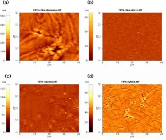
Figure 3. AFM images of pentacene layer spin- coated from different solvent. (measured rage is 40μm×40μm) (a) chlorobenzene (b) chloroform (c) toluene (d) p-xylene
hour to crystallization. For source/drain electrode, we used the Cr/Au double layer. Cr layer of 5 nm was deposited on the PVP insulator to improve adhesion of Au and gate insulator by e-beam sputtering system.
Au contacts of 100 nm were deposited by thermal evaporation. It is well known that gold is very good material of source and drain electrodes for OFTFs [17-18]. Before spin coating TIPS pentacene, hexa methyldi-silazane (HMDS) was spin coated for sur- face modification by spinner. The HMDS treatment
has already been known to enhance the hole mobility of pentacene-based OTFTs [19], in our research, we used the treatment to examine its effects on the channel/Source-Drain interface state. Finally, TIPS pentacene (1 wt%) with four different solvents:
chlorobenzene, p-xylene, chloroform and toluene, was spin coated on Source-Drain electrode.
Chloroform is a general solvent for OTFT's active layers. However, its low boiling point and rapid evaporation limit the time for crystallization during the spin-coating process. Chang et al., investigated a range of solvents with higher boiling points that is chloroform, thiophene, xylene, cyclohexylbenzene (CHB), and 1,2,4-trichlorobenzene (TCB) [20].
Table 1 is the chemical structure and physical properties of each solvent which was used as our TIPS pentacene solvent [21]. The OTFT device has bottom/top gate and bottom/top contact type structure. Our pentacene TFT device was made by bottom contact with Cr/Au as source and drain electrodes.
. Results & Discussion
Figure 2 is the optical microscopy image of the OTFT and boxed portion is spin-coated active layer where TIPS pentacene solvent was used as an active layer. Figure 3 shows the AFM image of the different TIPS pentacene solvent. 50 nm-thick pentacene thin-film on PVP was fabricated for AFM measurements. Each image range is 40 μm × 40 μm.
The grain size of pentacene layer is larger for sol- vents with higher boiling point.
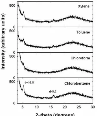
We can see the clear crystalline structure of pen- tacene thin film from Figure 4. TIPS pentacene film showed a preferential orientation of (001) direction.
The crystallinity of the film was strongly dependent
on the solvent. The TIPS pentacene film coated from
chlorobenzene solution showed the highest crystal-
Figure 4. XRD measurements of the pentacene layer formed by different solvent ((a) p-xylene (b) toluene (c) chloroform (d) chlorobenzene)
Figure 5. Transfer characteristics of TIPS pentacene OTFTs favricated with different solvent.
Figure 6. The transfer curves of an OTFT device fabricated with TIPS pentacene. The source-to-drain voltages were -40 V and -80 V respectively.
Figure 7. Output curves of an OTFT device fabricated with TIPS pentacene. The gate-to-source voltages were changed from 0 V to -80 V with -20 V step
linity, while the film coated from chloroform had nearly no crystalline phase.
In the figure 5, the best performance can be found in devices made by chlorobenzene. The entire cur- rent-voltage characteristics of our fabricated penta-
cene OTFTs were measured by a parameter analyzer (KEITHLEY 4200).
Figure 6 shows the logarithmic plot of I
dsand rep-
resents the properties of TIPS pentacene in the
Chlorobenzene. Then, Drain-Soure voltage bias is
-40 V, -80 V. And figure 7 shows the output charac-
teristics of an OTFT made with TIPS pentacene in
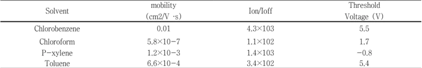
Solvent mobility
(cm2/V ·s) Ion/Ioff Threshold
Voltage (V)
Chlorobenzene 0.01 4.3×10³ 5.5
Chloroform 5.8×10⁻⁷ 1.1×10² 1.7
P-xylene 1.2×10⁻³ 1.4×10³ -0.8
Toluene 6.6×10⁻⁴ 3.4×10² 5.4
Table 2. The variation of electrical properties of pentacene OTFTs
chlorobenzene.
As clearly seen in the graph, the solvent of TIPS pentacene has significant effect on the electrical properties of OTFT device.
The field effect mobility and the threshold voltage V
thare extracted from saturation region of the transfer characteristic using the following equation.
Where I
dsis the drain current, L is the channel length, W is the channel width, C
iis the capacitance per unit area of the insulating layer, V
gs=-80 V is the gate voltage and V
this the threshold voltage. The in- sulator capacitance C
i= 6.5 nF/cm
2is a 600 nm thick insulator, and the device channel width W and length L are 2400 μm and 15 μm, respectively.
. Conclusion
Generally, grain size strongly depends on substrate temperature, deposition rate, and surface treatment.
Through experiment, we knew that grain size is also influenced by the solvent. Therefore we investigate a range of solvents with higher boiling points in this paper. With chlorobenzene as a solvent of higher boiling point, the device showed the highest satu- ration field-effect hole mobility of 1.0×10
-2cm
2/V·s, on/off ratio of 4.3×10
3and threshold voltage of 5.5 V. In contrast, chloroform with lower boiling point showed poor electrical properties with field-effect mobility of 5.8×10
-7cm
2/V·s, on/off ratio of 1.1×10
2and threshold voltage of 1.7 V. The electrical charac-
teristics of OTFT devise made with different solvent are listed in Table 2. We are unable to fully under- stand this phenomenon yet. However, we conclude that the solvent of pentacene film is not a unique in- dicator in determining the grain size.
Acknowledgement
This research was supported by a grant (F0004063) from the Information Display R&D Center, one of the 21st Century Frontier R&D Program funded by the Ministry of Commerce, Industry and Energy of the Korean Government.
References
[1] Y. Taur and T. H. Ning, Fundamentals of Modern VLSI Devices (Cambridge University Press, New York, 1988) p. 11.
[2] A. Tsumma, H. Koezuka, and T. Ando, Appl. Phys.
Lett. 49, 1210 (1986).
[3] G. Horowitz, Adv. Matter. 10, 365, (1998).
[4] H. E Katz and Z. Bao, J. Phys. Chem. B 104, 671 (2000).
[5] H. Sirrinbhaus, N. Tessler, and R. H. Friend, Science 280, 1741 (1998).
[6] A. Dodabalapur, Z. Bao, A. Makhija, J. G.
Laquindanum, V. R. Raju, Y. Feng, H. E. Katz, and J. Rogers, Appl. Phys. Lett. 73, 142 (1998).
[7] R. Wisnieff, Nature 394, 225 (1998).
[8] B.Comiskey, J. D. Albert, H. Yoshizawa, and J.
Jacobson, Nature 394, 253 (1998).
[9] N. K. Sheridon, U.S. Patent 4, 854 (1978).
[10] A. R. Brown, A. Pomp, C. M. Hart, and D. M.
de Leeuw, Science 270, 972 (1995).
[11] C. J. Drury, C. M. J Mutsaers, C. M. Hart, M.
Matters, and D. M. de Leeuw, Appl. Phys. Lett.
73, 108 (1998).
[12] Y. Y. Lin, A. Dodabalapur, R. Sarpeshkar, Z. Bao, W. Li, K. Baldwin, V. R. Raju, and H. E. Katz, Appl. Phys. Lett. 74, 2714 (1999).
[13] Y. Y. Lin, D. J. Gundlach, S. F. Nelson, and T.
N. Jackson, IEEE Trans. Electron Devices 44, 1325 (1997).
[14] T. N. Jackson, Y. Y. Lin, D. J. Gundlach, and H.
Klauk, IEEE J. Sel. Top. Quantum Electron. 4, 100 (1998).
[15] D. J. Gundlach, Y. Y. Lin, T. N. Jackson, S. F.
Nelson, and D. G. Schlom, IEEE Electron Device
Lett. 18, 87 (1997).
[16] Y. Y. Lin, D. J. Gundlach, S. F. Nelson, and T.
N. Jackson, IEEE Electron Device Lett. 18, 606 (1997).
[17] D.S. Kim, Y.S. Lee, H.H. Park, J.S. Choi, D.Y.
Kang, J. Kor. Vac. Soc., Vol. 9, No. 4. 379-381 (2000).
[18] S.H. Cho, S.H. Kim, N.-E. Lee, H.M. Kim, Y.W.
Nam, Thin Solid Films 475, 68 (2005).
[19] S.H. Cho, S.H. Kim, J.G. Lee, N.-E. Lee, Microelectron. Eng. 77, 116 (2005).
[20] Jui-Fen Chang, Baoquan Sun, Dag W. Breiby, Martin M. Nielsen, Theis I. Solling, Mark Giles, Iain McCulloch, and Henning Sirringhaus, Chem.
Mater., 16(23), pp.4772-4776 (2004).
[21] Samil Kho, Minsu Kim, Sunyoung Sohn, Donggeun
Jung, Jinhyo Boo, Seounghoon Jeong, Sanghee Ko
Park, J. Kor. Vac. Soc., Vol.14, No.4, 196 (2005)
용제에 따른 TIPS(triisopropylsilyl) Pentacene을 이용한 유기박막 트렌지스터의 전기적 특성에 관한 연구
김경석1,2, 김영훈1, 한정인1, 최광남2, 곽성관3, 김동식4, 정관수2
1
전자부품연구원 디스플레이연구센터, 분당 463-816
2
경희대학교 전자정보대학 전자공학과, 용인 446-701
3
유한대학 전자정보과, 부천 442-749
4