P1-12 / H. D. Hwang
• IMID 2009 DIGEST
Abstract
In this paper, we proposed a simple method of decreasing the off current generated by degradation for improve the electrical characteristics such as mobility and on/off current ratio by making the line patterns on the pentacene surface between the electrodes using atomic force microscope (AFM) lithography.
1. Introduction
Intensive interest in organic thin film transistors (OTFTs) owing to their simple and low-temperature process has expedited efforts to develop commercial applications for OTFTs in electronic devices, such as driving elements for flexible displays, RFID tags, and large-area sensor [1-3]. However, in spite of remarkable progress in device performances, OTFTs still suffer from the characteristic degradation by moisture and oxygen in air [4]. The H2O molecules in air makes the traps in pentacene layer that will be capturing charges in on state, leading to an increase in the conductivity between source and drain when the device is in off state and resulting in a decrease of the on/off current ratio [5]. Degradation by H2O molecules starts on the top surface of pentacene layer and slowly extends to the bottom of pentacene film [6].
In this paper, we made a line pattern to reduce the increasing of leakage current by degradation for maintenance of on/off current ratio by cutting off the current path in pentacene surface using atomic force microscopy (AFM). AFM based nanofabrication methods attract much interest for their ultra-high resolution, easy operation, and low equipment costs. AFM lithography methods are realized by using different interaction forces between the tip and the sample surface, such as physical, chemical and
mechanical forces. Because the curvature radius of AFM tip and the distance between the tip and the sample are both on the nano scale, local fields, such as force field and electric field, on the nano scale are generated. These local fields modify the sample surface and construct various nanostructures. AFM mechanical lithography makes scratch and indention on various material surfaces on the nano scale by applying a suitable force, and then nano patterns are obtained by controlling the movement of the tip.
2. Experimental
The device configuration of top contact OTFTs with line pattern was shown in Figure 1. Al layer of 70nm thickness for gate electrode was fabricated by thermal evaporation. The insulator, cross-linked poly(4-vilyphenol) (cPVP) was spin-coated with 350nm thick, which was confirmed by α-step profilemeter.
Fig. 1. The device configuration of OTFTs patterned by AFM.
We mixed the polymer PVP and the cross-linking agent poly(melamine-co-formalde-hyde) with the solvent propylene glycol monomethyl ether acetate
Reduction of Leakage current Generated by Degradation in
Organic Thin Film Transistors using Pattern on Pentacene
Surface by Atomic Force Microscope
Hyun Doo Hwang
1, Hyunsuck Kim
1, Chang Ho Kim
2and Jae-Hoon Kim
1,2*
1
Dept. of Electronics and Computer Engineering, Hanyang University, Seoul, Korea
2Research Institute of Information Display, Hanyang University, Seoul, Korea
Phone: +82-2-2220-0343 , E-mail: [email protected]
P1-12 / H. D. Hwang
IMID 2009 DIGEST •
(PGMEA). The pentacene purified by sublimation was thermally evaporated under pressure of 10-6 Torr. The thickness of the pentacene layer is 60nm, and the deposition rate was 0.5 Å/sec. The 400nm thick electrodes of gold were prepared. The channel length and width in our OTFTs were 50um and 300um, respectively. Atomic force microscopy lithography was performed using a PSIA XE-100 instrument. Diamond coated AFM probes (DT-NCHR) in contact mode were used during drew a line on the pentacene film (Fig. 2). This AFM probe was also in some cases used for imaging, but most of the AFM imaging was performed in non-contact mode using NCHR or NCLR probes.
Fig. 2. AFM images of line pattern on pentacene surface.
3. Results and discussion
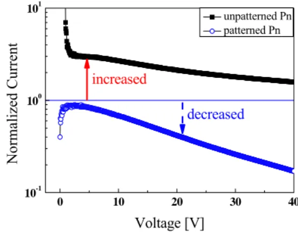
Figure 3 shows the comparison of current characteristics for the sample using oxidized pentacene with and without patterns in Insulator/Semiconductor/Metal (ISM) structure (i.e. the lines using AFM lithography). The slope in the I-V curve for patterned device is larger than without
pattern’s one. This phenomenon could be explained the pattern interrupt the current flow near the pentacene surface, as a result, the leakage current was decreased. 0 10 20 30 40 10-1 100 101 decreased unpatterned Pn patterned Pn N ormalized Current Voltage [V] increased
Fig. 3. Current versus voltage for leakage current in ISM structure.
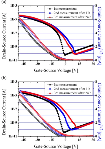
Figure 4 shows the transfer characteristics of OTFTs with and without pattern on pentacene surface. The chemical reaction between pentacene and H2O molecules induce free charge increasing the conductivity between source and drain on the surface of pentacene according to the time. The increased conductivity by degradation leads to gradually increase of leakage current shown in Figure 4(b). In contrast, a line pattern formed by AFM lithography with ~25nm depth reduced the leakage current increased by degradation by cutting off the current path in pentacene surface. The resistance of pentacene surface increased by a pattern, and the surface leakage current by degradation was decreased.
The threshold voltage shift to positive direction was caused by the electrical characteristics of degradation of cPVP insulator layer (Fig. 4) [7]. The bias stress was caused by water absorbed into the bottom dielectric layer far away from the conducting channel. The effect of absorbed water molecules is a slow change of the effective electric field during device operation that leads to the positive shift in threshold voltage.
P1-12 / H. D. Hwang • IMID 2009 DIGEST -45 -30 -15 0 15 30 1E-11 1E-9 1E-7 1E-5 1E-3 1st measurement 2nd measurement after 1 h 3rd measurement after 24 h Gate-Source Voltage [V] D rain-S our ce Cu rr ent [A ] (a) 0 2 4 6 8(Dr ain -S ou rc e C urren t) 1/2 [m A] -45 -30 -15 0 15 30 1E-11 1E-9 1E-7 1E-5 1E-3 1st measurement 2nd measurement after 1 h 3rd measurement after 24 h Gate-Source Voltage [V] Drain-Source Current [A] 0 2 4 6 8(Dr ain -S ou rc e C urren t) 1/2 [m A] (b)
Fig. 4. The electrical characteristics of OTFTs (a) with and (b) without pattern on pentacene surface.
4. Summary
We proposed the simple method to improve the electrical characteristics of OTFT using the lithography by AFM. We could decreased the surface leakage current by making the lines having enough depth and length on the pentacene surface between electrodes which have the perpendicular direction against electric field for improving the characteristics such as mobility and on/off ratio. Hereafter, additional experiments will be performed to analyze the electrical performance of OTFT for varying the depth, length, and numbers of lines.
Acknowledgement
This research was supported by a grant(F0004120-2008-31) from Information Display R&D Center, one of the 21st Century Frontier R&D Program funded by the Ministry of Knowledge Economy of Korean government.
5. References
1. S. R. Forrest, Nature, 428, p.911-918 (2004). 2. R. Rotzoll, S. Mohapatra, V. Olariu, R. Wenz, M.
Grigas and K. Dimmler, Appl. Phys. Lett., 88, p.123502 (2006).
3. L. Wang, D. Fine, S. I. Khondaker, T. Jung and A. Dodabalapu, Sens. Actuators, 113, p.539-544 (2000).
4. T. Jung, A. Dodabalapur, R. Wenz and S. Mohapatra, Appl. Phys. Lett., 87, p.182109 (2005).
5. Y. Qiu, Y. Hu, G. Dong, L. Wang, J. Xie and Y. Ma, Appl. Phys. Lett., 83, p.1644 (2003).
6. M. Ling, Z. Bao and D. Li, Appl. Phys. Lett., 88, p.033502 (2006).
7. T. N. Ng, J. H. Daniel, S. Sambandan, A. C. Arias, M. L. Chabinyc, and R. A. Street, J. Appl. Phys,