Journal of Navigation and Port Research International Edition Vol.34, No.7 pp. 539~542, 2010 (ISSN-1598-5725)
DOI : 10.5394/KINPR.2010.34.7.539
- 539 -
A Study on the EM Wave Absorber for Improving Electromagnetic Environment of Wireless LAN at 2.4 GHz
Gun-Suk Yoo*․†Dong-Il Kim․Dong-Soo Choi**․Dong Han Choi***
*,**,***,†Department of Radio Sciences and Engineering, Korea Maritime University, Busan 606-791, Korea
Abstract : In this paper, we designed and fabricated the Electro-Magnetic (EM) wave absorber for wireless LAN by using Amorphous and CPE. The material constants and the absorption properties were measured for the samples containing 50 %, 60 %, and 70 % weight fraction of Amorphous. Moreover, the EM wave absorption abilities were simulated for the EM absorbers in different thicknesses by adopting the measured permittivity and permeability, and then the EM wave absorber was fabricated based on the simulated design values. As a result, the EM wave absorber with the composition ratio in Amorphous : CPE = 60 : 40 wt.% with the thickness of 4 mm has the absorption ability more than 35 dB at 2.4 GHz. Thus, it is expected the wireless LAN environment can be improved by using the developed absorber.
Key words : EM wave absorber, CPE, wireless Lan, Amorphous, Absorption ability, material constant
* First Author : [email protected] 051)410-4932 †Corresponding author : [email protected] 051)410-4314 ** [email protected] 051)410-4932
*** [email protected], 051)410-4932
1. Introduction
With the rapid advancements in the electronics industry and the radio communication technology, mankind might enjoy his abundant life. On the other hand, serious social problems such as electromagnetic interference (EMI) and electromagnetic susceptibility (EMS), have arisen due to the increased applications of electromagnetic waves(Kim, et al., 1996). Therefore, the countermeasures against electromagnetic wave problems are important subjects(Kim, et al., 2006).
These problems can be solved through the use of EM wave absorbers. EM wave absorbers are well known to use three kinds of loss, conductive loss, dielectric lossesi, and magnetic loss(Choi, et al., 2003).
Wireless LAN is often applied at home or in office for several convenience merits. Frequency band of wireless LAN is 2.4 GHz and 5.2 GHz which are specified IEEE 802.11a and IEEE 802.11b(Stphen and Sailiga, 2000).
Wireless LAN environment in office has reflected waves that are caused by walls, ceilings, floors, and desks. It creates multi-path problems. Which reduce communication speed and lose data(Nitta, 2000). These problems can be solved by using the EM wave absorber.
In this paper, we fabricated the EM wave absorbers for wireless LAN using Sendust magnetic material inter-mixed with chlorinated polyethylene (CPE), and their impedances were measured. The complex relative permittivity
(ε&r=εr'−jεr'') and permeability (μ&r =μr'−jμr'') were
calculated by the measured data. The EM wave absorption abilities are simulated according to the thicknesses of the EM wave absorbers, and the EM wave absorber was manufactured based on the simulated design values.
2. Design of EM wave absorber
For an EM wave absorber made of a conductor-backed single layer type as shown in Fig. 1, the Return Loss (RL) can be obtained from the equivalent circuit as follows(Soh and Hashomoto, 2001, Pozer, 2005).
z [dB]
RL z
in in
ˆ 1 ˆ 1 log 20
10+
− −
=
(1) Here, is the normalized input impedance.
The normalized input impedance
zˆ
in is expressed as eq.(2) (Hashimoto, 1997).⎟ ⎠
⎜ ⎞
⎝
= ⎛
j dz r r
r
in r
ε μ
λ π ε
μ 2
ˆ tanh
(2) Where is the wavelength, d is the thickness of the sample, is the complex relative permittivity and is the complex relative permeability. The reflection-less condition
A Study on the EM Wave Absorber for Improving Electromagnetic Environment of Wireless LAN at 2.4 GHz
- 540 - for normal incidence of an electromagnetic wave is given by
Fig. 1 The single-layered EM wave absorber.
2 1
tanh ⎟ =
⎠
⎜ ⎞
⎝
⎛
j r rdr
r
ε μ
λ π ε
μ
(3)
Therefore, if the eq.(3) is solved the relationship between the material property and the sample thickness can be simulated. Further, it is possible to use equation (1) for confirmation of the absorption abilities(Choi, et al., 2006).
3. Preparation and Measurements of Samples
3.1 Sample for preparation
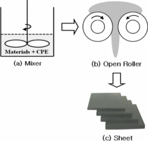
The conventional EM wave absorber is usually consisted of spinel structure Ferrite materials, such as Mn-Zn and Ni-Zn ferrites. According to Snoek’s limit, spinel structure ferrites have frequency limit at GHz rage because getting high permeability at high frequency rage is difficult(Snoek, 1984). Thus, we used Amorphous of soft magnetic metal powder and CPE as binder. The EM wave absorber was manufactured with process of Fig. 2.
Fig. 2 Fabricating process of an EM wave absorber.
First, Sendust was mixed with the binder of CPE, and the sheet-type absorber was fabricated using an open roller.
The open roller’s surface temperature was keeping 70℃
during sample preparation because the surface temperature affects the EM wave absorption ability of the sheet-type absorber(Moon, et al., 2003).
3.2 Measurement method
For the investigation of the EM wave absorption properties of the samples, the prepared sheet-type absorbers were punched into a toroidal shape with an inner diameter of 3.05 mm and an outer diameter of 6.95 mm. The absorption properties of the samples were investigated with the HP 8753D Vector Network Analyzer. Fig. 3 and 4 are diagrams of the measurement system used for the reflection coefficient and the sample holder, respectively.
Fig. 3 Measurement System for Reflection Coefficient
Fig. 4 A photo of EM wave absorber, Sample Holder and Sample
3.3 Measurements
We carried out the EM wave absorber design with the samples containing 50 wt.%, 60 wt.% and 70 wt.% of Amorphous. Fig. 5, 6 and 7 show reflection coefficients as a function of frequency for the samples containing difference composition ratios of materials. In Fig. 6, it is shown that
Gun-Suk Yoo․Dong-Il Kim․Dong-Soo Choi․Dong Han Choi
- 541 - the predictable optimum composition ratio of Amorphous is 60 wt.% at 2.4 GHz.
Fig. 5 Absorption ability of EM wave absorber (Amorphous : CPE = 50 : 50 wt.%)
Fig. 6 Absorption ability of EM wave absorber (Amorphous : CPE = 60 : 40 wt.%)
Fig. 7 Absorption ability of EM wave absorber (Amorphous : CPE = 70 : 30 wt.%)
4. Simulated and Measured results
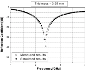
The material constants of these samples is calculated from the S-parameter of the samples using the ℓ-2ℓ method(Hashimoto, 1997). We simulated absorption ability of EM wave absorber using calculated material constants by MATLAB program. Absorption abilities of EM wave absorbers were simulated using the material constants by changing the thickness without changing the composition ratios. Figures 8 and 9 show the results. In Fig. 8 shows the absorption ability more than 15 dB with thickness 2.65 mm at 70 wt.% composition ratio. However, at the composition ratio of 60 wt.%, the absorption ability more than 35 dB was obtained the and thickness was 3.95 mm, which was the best results and, satisfies the target of this research.
Fig. 8 Simulated results of samples with different composition ratio at 2.4 GHz.
Fig. 9 Comparison of simulated and measured result.
A Study on the EM Wave Absorber for Improving Electromagnetic Environment of Wireless LAN at 2.4 GHz
- 542 -
5. Conclusion
According to simulation, the optimized composition ratio of Amorphous is 60 wt.%. They are shown in Fig. 9. The fabricated EM wave absorber by obeying the simulated results has over 35 dB absorption ability at 2.4 GHz.
Simulated and measured results agree well as shown in Fig.
9.
In the wireless LAN environment in office, there are so much reflected waves which occur from by walls, ceilings, floors, desks, and create multi-path problems. These problems can be eliminated by adopting EM wave absorbers.
In this paper, we investigated the EM wave absorber for improving the wireless LAN environment using Amorphous metal powder with CPE as binder. The material constants were calculated from the measured S-parameters. The absorption ability of the samples was also measured by the network analyzer and the absorption abilities of the samples were compared. The optimized composition ratio of the absorbing material was Amorphous : CPE = 60 : 40 wt.%, and the absorption ability of the EM wave absorber with thickness of 3.95 mm was 35 dB at 2.4 GHz. By using the developed absorber, it is expected to improve the wireless LAN environments.
Acknowledgment
This work was supported by the Fellowship Program of the Sanhak Foundation of Korea from Sept. 1, 2009 to Aug.
31, 2011.
References
[1] Choi, C. M., Kim, D. I., Li, R. and Ko, K. S.(2006),
"Development of the Electromagnetic Wave Absorber for 94 GHz Radar Sensors Using Permalloy", Inter. J.
KIMICS, vol.4, no.3, pp.114-117.
[2] Choi, D. H., Kim, D. I. and Song, J. M(2003),
“Dependence of Electromagnetic Wave Absorption Properties on Binders,” Journal of the Korean Physical Society, Vol. 42, No. 6, pp. 799-802.
[3] Hashimoto, O.(1997), Introduction to Wave Absorber, Morikita Shuppan.
[4] Kim, D. H., Kim, D. I., Choi, C. M. and Son, J. Y.(2006),
“A Study on Design and Fabrication of Complex Type EM Wave Absorber with Super Wide-band Characteristics," International Journal of Navigation and Port Research, Vol. 30, No. 2, pp. 161-166.
[5] Kim, D. I., Takahashi, M., Anzai, H. and Jun, S.
Y.(1996), "Electromagnetic Wave Absorber With Wide-Band Frequency Characteristics Using Exponentially Tapered Ferrite,” IEEE Trans. on EMC, Vol. 38, No. 2, pp. 173-177.
[6] Moon, S. H., Shin, S. J., Song, J. M. and Kim, D.
I.(2003), "Development of composite Ba ferrite EM wave absorbers for GHz frequency", J. Korea Electromagnetic Engineering Soc., vol. 14, no. 12, pp.
1329-1334.
[7] NITTA, S.(2000), "The Future of EMC Technology", IEICE Trans. Commun, vol. E83-B, no. 3.
[8] Pozer, D. M.(2005), Microwave Engineering - 3rd ed., J.
Wiley & Sons.
[9] Snoek, J. L(1984), "Dispersion and Absorption in Magnetic Ferrite at Frequency above one Mc/s", physical, vol. 14, pp. 207-217.
[10] Soh, T., Hashomoto, O.(2001), "A Study on Millimeter-Wave Absorber coating for V Band and W Band", Trans. IEICE J84-B, pp. 1523-1528.
[11] Stphen V., Sailiga, Ph. D.(2000), "An Introduction to IEEE 802.11 Wireless LANs", Radio Frequency Integrated Circuits(RFIC) Symposium.
Received 27 May 2010 Revised 15 August 2010 Accepted 17 August 2010