The geometry change of carbon nanofilaments by SF
6incorporation in a thermal chemical vapor deposition system
Sung-Hoon Kim
†Department of Engineering in Energy & Applied Chemistry, Silla University, Busan 617-736, Korea (Received May 26, 2011)
(Revised June 3, 2011) (Accepted June 10, 2011)
Abstract Carbon nanofilaments (CNFs) could be synthesized on nickel catalyst layer-deposited silicon oxide substrate using C2H2 and H2 as source gases under thermal chemical vapor deposition system. By the incorporation of SF6 as a cyclic modulation manner, the geometries of carbon coils-related materials, such as nano-sized coil and wave-like nano- sized coil could be observed on the substrate. The characteristics (formation density and morphology) of as-grown CNFs with or without SF6 incorporation were investigated. Diameter size reduction for the individual CNFs-related shape and the enhancement of the formation density of CNFs-related material could be achieved by the incorporation of SF6 as a cyclic modulation manner. The cause for these results was discussed in association with the slightly increased etching ability by SF6 addition and the sulfur role in SF6 for the geometry change.
Key words Carbon nanofilaments, Carbon coil, SF6, Geometry, Cyclic modulation process, Thermal chemical vapor deposition
1. Introduction
Carbon nanofilaments (CNFs), called carbon nanotubes if hollow and carbon nanofibers if filled, would be use- ful for the elements of nanoelectronic devices due to their fascinating shape of the micrometer scale length and the nanometer scale diameter [1, 2]. Helical carbon coils, as an eccentric shape of carbon nanofilaments, were also regarded to have promising materials characteristics [3, 4].
Basically, helically coiled carbon nanotubes were known to be constructed by periodically inserting heptagonal and pentagonal rings into hexagonal network [5]. The electrical properties of CNFs or helically coiled carbon nanotubes may be metallic, semiconducting or semi-metal- lic depending on their geometry including diameter and the pentagonal and heptagonal rings placement in car- bon coils [6]. Therefore the controlled geometry of CNFs would be essential to achieve the controlled elec- trical properties of CNFs.
For the synthesis techniques of carbon nanofilaments, various methods have been introduced, such as arc-dis- charge [7], pyrolysis [8], laser ablation [9], plasma or thermal chemical vapor deposition methods [10, 11], and so forth. Among these techniques, thermal chemical vapor deposition (TCVD) technique using the metal catalyst has
been more noticed because of its relative inexpensive and applicable feature. In addition, the enhancement of carbon nanofilaments having the controlled-geometry (diam- eter, shape, and so on) would be indispensible for the practical application of carbon nanofilaments. Recently, we have introduced an in-situ cyclic on/off modulation process of C
2H
2/H
2flow to enhance the formation yield of CNFs [12]. It can be simply achieved by turning a source gas flow rate in a reaction system on or off dur- ing the initial deposition stage. For the metal catalyst used in TCVD, iron family (Fe, Co, Ni), especially Ni, were known to be effective catalysts for the formation of carbon nanofilaments [13, 14].
This work presents the variation of carbon filaments geometries by the incorporation of SF
6in source gases (C
2H
2/H
2) during the initial deposition stage. To enhance the formation yield of carbon nanofilaments, we applied the gas composition cycling technique for C
2H
2, H
2and SF
6. The variation of the as-grown CNFs characteristics according to the different catalysts, namely the formation density and the geometry, was examined and discussed.
2. Experimental
The SiO
2substrates in this work were prepared by the thermal oxidation of the 2.0 × 2.0 cm
2p-type Si (100) substrates. The thickness of silicon oxide (SiO
2) layer on Si substrate was estimated about 300 nm. To form Ni
†Corresponding author
†Tel: +82-51-999-5619
†Fax: +82-51-999-5335
†E-mail: [email protected]
of these gases flows during the initial deposition stage.
According to the different reaction processes, the flows of source gases were the continual H
2+ C
2H
2flow and the iterative orders of the procedures. Namely,
Process I: Continual H
2+ C
2H
2flow Process II: H
2+ C
2H
2flow → H
2+ SF
6flow
Process II:→ H
2+ C
2H
2flow → H
2+ SF
6flow
Process II:→ H
2+ C
2H
2flow.
Carbon species to form CNFs are generated from H
290 min, respectively. The C
2H
2flow on/off time ratio was set as 180/30 s. So, the interval time for one cyclic was 3.5 minutes and the numbers of cycles were 2 times. The total cyclic modulation time was 7 minutes. The detailed reaction conditions according to the different processes with samples were shown in Table 1.
Detailed morphologies of CNFs-deposited substrates were investigated by using field emission scanning elec- tron microscopy (FESEM).
3. Results and Discussion
Fig. 2 shows FESEM images showing the surface mor- phologies for sample A (without SF
6incorporation case).
To compare the formation density of CNFs, the outermost side (Figs. 2a and c) and center (Figs. 2b and d) positions on the samples were chosen for investigation using FESEM. As shown in Fig. 2, CNFs-related materials including embryos could be well-developed irrespective of the position on the sample. Furthermore, the CNFs forma- tion density seems to be not much different according to the position on the sample. As shown in high-magnified FESEM images (Figs. 2c and d), the embryo for CNFs formation and the immature CNFs could be observed.
Fig. 3 shows FESEM images showing the surface mor- phologies for sample B (with SF
6incorporation case).
The CNFs formation aspect and density according to the position on the sample are not much different from the case of Fig. 2. In this case, however, the change of CNFs geometry from a conventional linear type to a nano-sized coil-like type could be clearly observed by the incorpo-
Table 1Experimental conditions for the deposition of CNFs on the substrates for samples A and B
Processes
Conditions0
Samples
C2H2 flow rate (sccm)
H2 flow rate (sccm)
SF6 flow rate (sccm)
Total pressure (Torr)
Total deposition time (min)
Cyclic on/off modulation
of source gases flow (sec) Number of cycles (No.)
Total cyclic process time (min)
Substrate temperature (oC) C2H2 H2 SF6
I Sample A 35 15 0 125 90 - - - 0 0 750
II Sample B 35 15 35 125 90 180/30 - 30/180 2 7 750
Fig. 1. Different reaction processes: the steady process (pro- cess I: sample A) and the cyclic process having SF6+ H2 as
etching components (process II: sample B).
ration of SF
6as a cyclic modulation manner (compare Figs. 2 with 3). In general, many types of carbon coils- related geometries could be observed on sample surfaces, so they could be usually classified into four geometrical categories, namely linear tub (LT), micro-sized coil (MC), nano-sized coil (NC), and wave-like nano-sized coil (WNC) (see Fig. 4). In this case, nano-sized coil (NC) and wave- like nano-sized coil (WNC) could be mostly observed as shown in high-magnified FESEM images (see Fig. 3).
Carbon coils formation densities were mainly measured using several 50k magnified FESEM images. For objec-
tively measuring carbon coils formation density, image analyzing method has been developed by placing square- graphed transparent paper onto the enlarged copies of FESEM images. Under the assumption of monolayer- grown carbon coils formation on the substrate, the occupied areas by various type carbon coils including embryos with or without the incorporation of SF
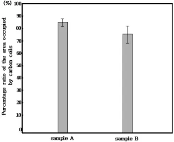
6as a cyclic modulation manner were measured as shown in Fig. 5.
The y-axis represents the percentage ratio of the area occupied by carbon coils. The analysis showed that the average occupied area of carbon coils with SF
6incorpo- ration was about 113% for that without SF
6incorpora- tion. In addition, the incorporation of SF
6as a cyclic modulation manner in the source gases seems to reduce the diameter size of the individual CNFs (comparing
Fig. 4. Various shapes of carbon coils-related geometries. In generally, many types of carbon coils-related geometries could be mainly classified into four geometrical categories, namely linear tub (LT), micro-sized coil (MC), nano-sized coil (NC),and wave-like nano-sized coil (WNC).
Fig. 3. FESEM images of CNFs-deposited substrate for sam- ple B (a) at the outermost side and (b) center positions on the substrate and their magnified images (c) at the outermost side
and (d) center positions on the substrate.
Fig. 5. The occupied areas by various type carbon coils with (sample A) or without (sample B) SF6 incorporation as a cyclic modulation manner. It was measured under the assumption of
monolayer-grown carbon coils formation on the substrate.
Fig. 2. FESEM images of CNFs-deposited substrate for sam- ple A (a) at the outermost side and (b) center positions on the substrate and their magnified images (c) at the outermost side
and (d) center positions on the substrate.
CNFs-related shape images of Figs. 2 with 3). Conse- quently, the number density of the individual CNFs would be much higher at sample B.
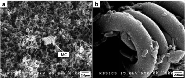
Occasionally, a couple of micro-sized carbon coils could be observed on the surface of the substrate as shown in Fig. 6. Diameters of the micro-sized carbon coils and the composed carbon nanofilaments are in the range of several micrometers and a few hundred nanometers, respectively.
The length range of the coil are in the range between a few micrometers and a few tens micrometers.
Based on the results shown in Figs. 2~6, we propose that the incorporation of SF
6as a cyclic modulation man- ner could give rise to the change of CNFs geometry from a conventional linear type to a nano-sized coil-like type. In addition, a reduction of the diameter size of the individual CNFs as well as the enhancement of CNFs- related materials formation density could be achieved by the incorporation of SF
6as a cyclic modulation manner.
The cause for these results was considered to be due to the slightly increased etching ability by SF
6addition to H
2gas concentration during the etching time in the cyclic modulation process. It may facilitate the suitable CNFs nucleation sites. Furthermore, it may etch away the superfluous materials of the as-grown CNFs. Consequently the diameter size of the as-grown CNFs would be reduced by SF
6addition. The change of CNFs geometry from a conventional linear type to a nano-sized wave-like coil type seems to be due to the sulfur role in SF
6as previous reports [15, 16].
4. Conclusions
The CNFs geometry change from conventional linear
type to nano-sized coil-like type could be achieved by the incorporation of SF
6as a cyclic modulation manner.
Diameter size for the individual CNFs-related shape could be reduced by the cyclic on/off modulation pro- cess of C
2H
2/H
2flow. In addition, the SF
6incorporation in the cyclic process could promote the formation density of CNFs-related material. The cause for these results was considered to be due to the slightly increased etch- ing ability by SF
6addition to H
2gas concentration dur- ing the etching time in the cyclic modulation process.
The change of CNFs geometry from a conventional lin- ear type to a nano-sized coil-like type seems to be due to the sulfur role in SF
6References
[ 1 ] S.J. Tans, M.H. Devoret, H. Dai, A. Thess, R.E. Sma- ley, L.J. Geerligs and C. Dekker, “Individual single-wall carbon nanotube as quantum wires”, Nature 386 (1997) 474.
[ 2 ] L. Marty, V. Bouchiat, A.M. Bonnot, M. Chaumont, T.
Foutnier, S. Decossas and S. Roche, “Batch processing of nanometer-scale electrical circuitry based on in-situ grown single-walled carbon nanotubes”, Microelec- tronic Engineering 61-62 (2002) 485.
[ 3 ] L.J. Pan, T. Hayashida, M. Zhang, Y. Nakayama, “Field emission properties of carbon tubule nanocoils”, Jpn. J.
Appl. Phys. 40 (2001) L235.
[ 4 ] S. Amelinckx, X.B. Zhang, D. Bernaerts, X.F. Zhang, V.
Ivanov and J. B. Nagy, “A formation mechanism for catalytically grown helix-shaped graphite nanotubes”, Science 265 (1994) 635.
[ 5 ] A. Fonseca, K. Hernadi, J.B. Nagy, Ph. Lambin and A.
Lucas, “Growth mechanism of coiled carbon nano- tubes”, Carbon 33 (1995) 1759.
[ 6 ] K. Akagi, R. Tamura and M. Tsukada, “Electronic struc- ture of helically coiled cage of graphitic carbon”, Phys.
Fig. 6. FESEM images of the CNFs-deposited substrate for sample B (a) at the center position on the substrate and (b) its magnified image. Occasionally, a couple of micro-sized carbon coils could be observed on the surface of the substrate.
Rev. Lett. 74 (1995) 2307.
[ 7 ] D.S. Bethune, C.H. Kiang, M.S. Devries, G. Gorman, R.
Savoy, J. Vazquez and R. Beyers, “Cobalt-catalyzed growth of carbon nanotubes with single-atomic-layer walls”, Nature 363 (193) 605.
[ 8 ] M. Terrones, N. Grobert, J. Olivares, J.P. Zhang, H. Ter- rones, K. Kordatos, W.K. Hsu, J.P. Hare, P.D. Townsend, K. Prassides, A.K. Cheetham, H.W. Kroto and D.R.M.
Walton, “Controlled production of aligned-nanotube bun- dles”, Nature 388 (1997) 52.
[ 9 ] A. Thess, R. Lee, P. Nikolaev, H. Dai, P. Petit, J. Rob- ert, C. Xu, Y.H. Lee, S.G. Kim, A.G. Rinzler, D.T. Col- bert, G.E. Scuseria, D. Tomanek, J.E. Fisher and R.E.
Smalley, “Crystalline ropes of metallic carbon nano- tubes”, Science 273 (1996) 483.
[10] W.Z. Li, S.S. Xie, L.X. Qain, B.H. Chang, B.S. Zou, W.Y. Zhou, R.A. Zhao and G. Wang, “Large-scale syn- thesis of aligned carbon nanotubes”, Science 274 (1996) 1701.
[11] Z.F. Ren, Z.P. Huang, J.W. Xu, J.H. Wang, P. Bush,
M.P. Sigal and P.N. Provencio, “Synthesis of large arrays of well-aligned carbon nanotubes on glass”, Sci- ence 282 (1998) 1105.
[12] K.-D. Kim, S.-H. Kim, N.S. Kim and D.-U. Kim, “Effect of the on/off cyclic modulation time ratio of C2H2/H2 flow on the low temperature deposition of carbon nanofilaments”, J. Nanosci. Nanotechnol. 7 (2007) 3969.
[13] A. Moisala, A.G. Nasibulin and E.I. Kauppinen, “The role of metal nanoparticles in the catalytic production of single-walled carbon nanotubes-a review”, J Phys: Con- dens Matter 15 (2003) S3011.
[14] A.C. Dupuis, “The catalyst in the CCVD of carbon nan- otubes-a review”, Prog. Mater. Sci. 50 (2005) 929.
[15] X. Chen and S. Motojima, “Morphology of the growth tip of carbon microcoils/ nanocoils”, Carbon 37 (1999) 1817.
[16] S. Motojima, S. Asakura, T. Kasemura, S. Takeuchi and H. Iwanaga, “Electrical properties of carbon micro coils”, Carbon 34 (1996) 289.