http://dx.doi.org/10.5369/JSST.2016.25.5.326 pISSN 1225-5475/eISSN 2093-7563
Digital CMOS Temperature Sensor Implemented using Switched-Capacitor Circuits
Bich Son
1, Byeong-Jun Park
1, Gwang-Hoe Gu
1, Dae-Eun Cho
2, Hueon-Beom Park
1, and Hang-Geun Jeong
1Abstract
A novel CMOS temperature sensor with binary output is implemented by using fully differential switched-capacitor circuits for resis- torless implementation of the temperature sensor core. Temperature sensing is based on the temperature characteristics of the pn diodes implemented by substrate pnp transistors fabricated using standard CMOS processes. The binary outputs are generated by using the charge-balance principle that eliminates the division operation of the PTAT voltage by the bandgap reference voltage. The chip was designed in a MagnaChip 0.35-µm CMOS process, and the designed circuit was verified using Spectre circuit simulations. The verified circuit was laid out in an area of 950 µm×557 µm and is currently under fabrication.
Keywords: Temperature sensor, CMOS, Switched-capacitor, Charge-balance, Sigma-delta modulation
1. INTRODUCTION
CMOS temperature sensors with digital output are attractive due to the advantages of low cost and ease of the digital controller user interface. Most CMOS temperature sensors are based on the temperature characteristics of the pn diode [1-3]. A proportional- to-absolute temperature (PTAT) voltage can be readily generated by taking the voltage difference between the two diodes forward- biased at different current densities. The forward-biased diode voltage has complementary-to-absolute temperature (CTAT) characteristic, which is needed to compensate for the PTAT characteristic to obtain the reference voltage required for measurement.
In this paper, we present a novel digital CMOS temperature sensor implemented by fully differential switched-capacitor circuits. The temperature sensing diodes are implemented by the substrate pnp transistors fabricated using a standard CMOS
process. Switched-capacitor circuits are used to minimize the use of resistors that can lead to an increased power consumption at low resistance and an increased chip area at high resistance.
To simplify the hardware, the digital output is obtained by using the charge-balance principle [3]. The complete temperature sensor was designed using a 0.35-μm CMOS process. The designed circuit is currently under fabrication after verification using Cadence Spectre.
This paper is organized as follows. Section 2 discusses the operating principles of the designed temperature sensor. The circuit designs of the major blocks are covered in Section 3. The most important sub-block used in most of the blocks is the OTA.
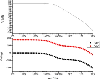
The design of a fully differential folded cascode OTA is discussed in Section 4. Section 5 shows the verification results obtained by circuit simulations. Finally, conclusions are given in Section 6.
2. PRINCIPLE OF OPERATION
2.1 Temperature sensing
The starting equation is the approximate current-voltage (I D – V D ) relationship of the forward-biased pn diode as expressed in (1).
, (1)
where I S is the saturation current of the diode, whereas q, k, and T are the electronic charge, Boltzmann constant, and absolute temperature, respectively.
I
DI
Se
qVD ---kT
≈
1
Department of Electronic Engineering, Chonbuk National Unversity College of Engineering, Chonbuk National University, 567 Baekje-daero, Deokjin-gu, Jeollabuk-do 561-756, Korea
2
Major of Semiconductor Science and Technology, Chonbuk National Unversity
College of Natural Science, Chonbuk National University, 567 Baekje-daero, Deokjin-gu, Jeollabuk-do 561-756, Korea
+
Corresponding author: [email protected] (Received: Sep. 23, 2016, Accepted: Sep. 30, 2016)
This is an Open Access article distributed under the terms of the Creative Commons Attribution Non-Commercial License(http://creativecommons.org/
licenses/bync/3.0) which permits unrestricted non-commercial use, distribution,
and reproduction in any medium, provided the original work is properly cited.
From (1), the diode voltage can be solved as shown in (2):
(2)
In (2), the diode voltage seems to be a PTAT voltage, but it turns out to be a CTAT voltage as will be discussed below. This is because I S is a rapidly increasing function with temperature.
However, if we take the difference between the two diode voltages with different current densities, the resulting difference in voltage can be expressed as in (3).
, (3)
where p is the current density ratio.
In (3), we can see that the difference voltage is a PTAT voltage that depends on the physical constants and the current density ratio. Thus, the difference voltage is fairly independent of the process and supply voltage variations.
To understand why the diode voltage is a CTAT voltage, let us examine the temperature dependence of the saturation current that can be expressed as in (4).
, (4)
where A, n i , m p , and G B are the diode area, intrinsic carrier density, carrier mobility, and Gummel number, respectively.
If the temperature dependencies of the intrinsic carrier density and the mobility are substituted into (4), we obtain (5).
, (5)
where η is approximately 2.5 and V go is the bandgap voltage extrapolated to T = 0 K, which is approximately 1.2 V.
Now we can solve (5) for the diode voltage to obtain (6).
(6)
It is more convenient to express the diode voltage with respect to some reference temperature, T r , as in (7).
(7) The temperature dependence of the diode current can be expressed as in (8),
(8)
If we substitute (8) into (7), we obtain (9).
(9)
If we neglect the nonlinear logarithmic term, the diode voltage expression can be simplified to (10).
(10)
Note that (10) shows that the diode voltage is a CTAT voltage, since the bandgap voltage is greater than the diode voltage. If we set the reference temperature as 300 K and assume that the diode voltage is 600 mV, (10) gives a temperature coefficient of -2 mV/ o C. Let us define the diode voltage as V CTAT . Now this negative coefficient of V CTAT can be compensated for by adding a PTAT voltage, V PTAT , properly scaled by 2 mV/ o C, to generate the bandgap reference voltage, V BGR , which has a value of 1.2 V and virtually independent of the process, voltage and temperature variations.
2.2 Sigma-delta conversion for digital readout
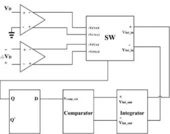
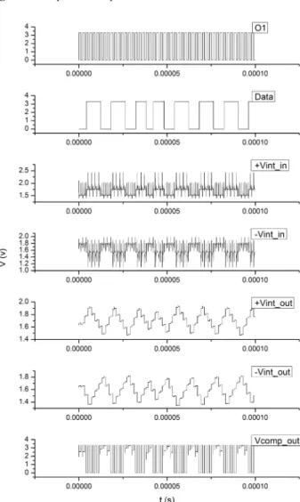
Now we can determine the temperature by taking the ratio of V PTAT to V BGR . The ratio changes from 0 to 1 as the absolute temperature increases from 0 K to 600 K, with its practical validity restricted to part of the entire range. A division operation is needed to obtain the ratio. The division operation can be eliminated if we use a charge-balance-based analog-to-digital conversion. The charge balance is achieved by the combined action of the integrator and the comparator shown in Fig. 1, resulting in almost equal amounts of charge flow into and out of the capacitor in the integrator on the average [3]. Note that the density of “1” in the sigma-delta modulated data should be proportional to the temperature. Since V PTAT increases with the temperature and V PTAT decreases with the temperature, the charge balance can be expressed as in (11). In this implementation, V CTAT is subtracted from the accumulated output for the data of “1”, while V PTAT is added to the accumulated output for the data of “0”.
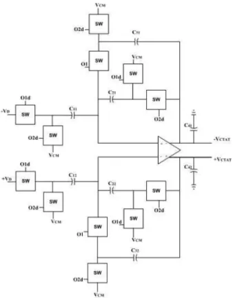
(11) Resistive loads are difficult to drive using CMOS circuits. To minimize the use of resistors, the required amplifiers and integrator are implemented by using switched capacitor circuits.
V
DkT --- q I
DI
S⎝ ⎠ ---- ln ⎛ ⎞
=
V
D≡ V
D2– V
D1Δ kT
--- q ln ( ) p
=
I
SkTAn
i2μ
pG
B---
=
I
D( ) CT T
ηe
q V[ D( ) VT– η0] ---kT