Journal of the Microelectronics & Packaging Society http://dx.doi.org/10.6117/kmeps.2013.20.4.065 Vol. 20, No. 4, p. 65-68. 2013
65
Maskless Screen Printing Process using Solder Bump Maker (SBM) for Low-cost, Fine-pitch Solder-on-Pad (SoP) Technology
Kwang-Seong Choi
†, Haksun Lee, Hyun-Cheol Bae and Yong-Sung Eom IT Materials and Components Laboratory
Electronics and Telecommunications Research Institute, Daejeon 305-700, Korea (Received September 13, 2013: Corrected September 30, 2013: Accepted December 2, 2013)
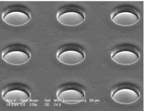
Abstract: A novel bumping process using solder bump maker (SBM) is developed for fine-pitch flip chip bonding. It features maskless screen printing process. A selective solder bumping mechanism without the mask is based on the material design of SBM. Maskless screen printing process can implement easily a fine-pitch, low-cost, and lead-free solder- on-pad (SoP) technology. Its another advantage is ternary or quaternary lead-free SoP can be formed easily. The process includes two main steps: one is the thermally activated aggregation of solder powder on the metal pads on a substrate and the other is the reflow of the deposited powder on the pads. Only a small quantity of solder powder adjacent to the pads can join the first step, so a quite uniform SoP array on the substrate can be easily obtained regardless of the pad configurations. Through this process, an SoP array on an organic substrate with a pitch of 130 µm is, successfully, formed.
Keywords: Maskless screen printing process, Solder bump maker (sbm), Solder-on-pad, Lead-free solder, Fine-ptich, Thermally actived aggegation
1. Introduction
Flip chip technology becomes one of the most popular interconnection technologies in the packaging industry because of it cost-effectiveness in the 200 to 700 pin count range.
1)Its application area covers the conventional packaging technologies such as ball grid array (BGA), wafer level packaging (WLP), and the emerging technologies like 2.5D and 3D IC integration. Solder-on-pad (SoP) technology was introduced to obtain a higher standoff height than the conventional surface finishes used for flip-chip substrates in order to increase the manufacturability and reliability of the fine-pitch flip chip bonding with pitch less than 150 µm.
2)The proposed SoP technologies were stencil printing, solder jetting, controlled collapse chip connection new process (C4NP), electro-plating, micro-ball placement, super solder, and so on. Each technology has its own disadvantages such as compatibility with fine-pitch, expensive equipment, low throughput, and environmental problems.
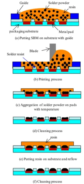
In this paper, we propose a novel bumping process using solder bump maker (SBM) for a fine-pitch, lowcost, and lead-free solder-on-pad (SoP) technology. SBM is based on the rheological behavior of the solder powder in resin.
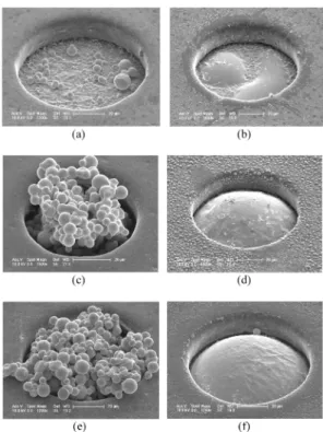
3-8)Since we uses solder powder commercially available for SBM, the solder bump array formed using SBM can have easily ternary or quaternary lead-free composition, which is necessary for the reliability of the solder joints of the fine- pitch flip chip bonding. The SoP technology based on SBM features a maskless screen printing process so that it can be applied to finer-pitch flip chip bonding less than 150 µm, which was difficult for the conventional printing process using a mask and solder paste. The process is composed of two major steps. First, using SBM, solder is deposited on the pads on a substrate with an increase in temperature. The peak temperature of this step is just below the melting point of the solder used in the SBM. Second, the reflow of the deposited solder forms SoP. The first step is thermally activated process depending on the peak temperature of the temperature profile and the amount of the deoxidizing agent in the SBM. Here, the effect of the variations of the amount the deoxidizing agent on the volume of SoP was investigated to find out the mechanism of the solder deposit process. Test vehicles with a pitch of 130 µm were prepared, and uniform SoP arrays with Sn3.0Ag0.5Cu (SAC305) on the substrates were achieved.
†