• 검색 결과가 없습니다.

Improvement on Surface and Electrical Properties of Polymer Insulator Coated TiO<sub>2</sub> Thin Film by Atomic Layer Deposition

N/A
N/A
Protected

Academic year: 2021

Share "Improvement on Surface and Electrical Properties of Polymer Insulator Coated TiO<sub>2</sub> Thin Film by Atomic Layer Deposition"

Copied!
5
0
0

로드 중.... (전체 텍스트 보기)

전체 글

(1)

전기적 특성의 향상

김남훈

1

, 박용섭

2,a


1 조선대학교 전기공학과

2 조선이공대학교 전자과

Improvement on Surface and Electrical Properties of Polymer Insulator Coated TiO 2

Thin Film by Atomic Layer Deposition

Nam-Hoon Kim

1

and Yong Seob Park

2,a

1 Department of Electrical Engineering, Chosun University, Gwangju 61452, Korea

2 Department of Electronics, Chosun College of Science and Technology, Gwangju 61453, Korea

(Received June 2, 2016; Revised June 12, 2016; Accepted June 13, 2016)

Abstract: Titanium oxide (TiO

2) thin films were synthesized on polymer insulator and Si substrates by atomic layer deposition (ALD) method. The surface and electrical properties of TiO2 films synthesized at various ALD cycle numbers were investigated. The synthesized TiO2 films exhibited higher contact angle and smooth surface. The contact angle of TiO2 films was increased with the increase of ALD-cycle number. Also, the rms surface roughness of films was slightly rough with the increase of ALD-cycle number. The leakage current on TiO2 film surface synthesized at various conditions were uniformed, and the values were decreased with the increase of ALD-cycle number. In the results, the performance of TiO2 films for self-cleaning critically depended on a number of ALD-cycle.

Keywords: TiO

2, Atomic layer deposition (ALD), Contact angle, Leakage current, Rms surface roughness

1. 서 론

높은 유전상수(dielectric constant), 가시광선에서 우수한 투명도와 굴절률(refractive index)을 가지는 titanium dioxide(TiO

2

) 박막은 매우 뛰어난 광촉매 활성도를 가지고 있어 플렉서블 디스플레이, 태양전지

a. Corresponding author; [email protected]

Copyright ©2016 KIEEME. All rights reserved.

This is an Open-Access article distributed under the terms of the Creative Commons Attribution Non-Commercial License (http://creativecommons.org/licenses/by-nc/3.0) which permits unrestricted non-commercial use, distribution, and reproduction in any medium, provided the original work is properly cited.

와 화학 센서 등에 이용되고 있다 [1-3]. 반도체 등

다양한 분야에서 잠재력을 지닌 TiO

2

박막은 원자층 증

착(atomic layer deposition, ALD), 라디오파 스퍼터링

법(radio-frequency sputtering; RF sputtering), 졸겔

(sol-gel process), 화학기상 증착(chemical vapor

deposition, CVD) 등 여러 방법으로 제작되고 있다

[4-7]. 이러한 제작 방법 중 원자층 증착 방법은 개

별적으로 분리된 반응 기체들이 펄스형태로 반응기에

공급되어 기판 표면에서 표면 포화 반응에 의해 박 막

(2)

(a) (b)

(c) (d)

Fig. 1. Contact angle shapes of TiO

2

thin films synthesized on polymer insulator with various number of ALD-cycles; (a) 250, (b) 500, (c) 750, and (d) 1,000 cycles.

형성이 가능하기 때문에 정확한 두께 및 조성 제어가 가능하며, 특히 복잡한 형상의 기판 위에서도 실제의 형상과 유사한 단차 도포성(step coverage)을 구현할 수 있다 [8,9]. 자기세정 특성은 150

o

이상의 접촉각 을 유지하며, 물방울 크기의 적절한 요철 등으로 낮은 자유에너지의 소수성 표면을 가지고 있어야 가능하게 되는데, 광촉매 소재로서 TiO

2

SiO

2

, ZnO, WO

3

등의 소재들은 연구되어지고 있다. 본 연구에서 이 소재 중 강력한 산화 분해력을 가지며 초친수 특성과 산과 염 기에 대한 화학적인 안정성을 보유하고 있는 TiO

2

소 재에 대한 연구를 진행하였으며 [10,11], TiO

2

박막 표면의 극 친수 또는 극 소수 특성을 활성화하여 광촉 매 특성을 향상시키며, 표면 오염원으로부터 완벽한 독립을 위해 화학 결합에 의해 박막을 합성할 수 있는 원자층 증착 장치를 사용하였다. 또한 TiO

2

박막의 표 면 특성과 전기적 특성 변화를 위한 변수로 TiO

2

박막 의 두께를 선택하였으며, ALD 시스템에서 두께 변수 는 온도변수와 같이 박막의 결정성 및 구조, 표면 특 성을 결정하는 주요 변수로서 박막의 두께 조절을 위 해 ALD 사이클 주기를 선택하였다 [12].

2. 실험 방법

TiO

2

박 막 은 실 리 콘 과 폴 리 머 절 연 체 (polym er

(a) (b)

(c) (d)

250 500 750 1000

105 110 115 120 125

C o n ta c t a n g le v a lu e [

o

]

Number of ALD-Cycles

Fig. 2. Contact angle shapes of TiO

2

thin films synthesized on silicon substrate with various number of ALD-cycles; (a) 250, (b) 500, (c) 750, (d) 1,000 cycles, and contact angle value of TiO

2

films as a function of number of ALD-cycles.

insulator) 기판 위에 원자층 증착(atomic layer deposition, ALD) 장치를 이용하여 합성하였으며, TTIP (titanium-tetra-isopropoxide: (Ti(OCH(CH3)2)4))를 전 구체로 사용하였으며, 물(H

2

O)을 반응기체로 사용하였다.

또한, 고순도 질소(99.99%)를 퍼징가스로 사용하였다.

기본 압력은 3 mTorr 이하로 하였으며, 증착 도중에

도 충분한 퍼징을 위해 10 mTorr 미만의 압력을 유

지하였다. TTIP의 온도는 50℃ 정도로 유지하였으며,

물의 온도는 상온이다. TiO

2

박막의 두께 조절을 위해

ALD 시스템에서 사이클 주기를 변수로 사용하였으며,

사이클 주기는 250부터 1,000까지 250을 차이로 두어

설정하였다. 두께에 따라 실리콘 기판위에 합성되어진

TiO

2

박막의 표면과 자기세정 특성, 그리고 박막의 전

기적 특성들은 field emission scanning electron

(3)

성들을 고찰하였다.

3. 결과 및 고찰

그림 1은 ALD 사이클 주기에 따라 폴리머 절연체 기판위에 합성되어진 TiO

2

박막의 표면에서의 자기세 정 특성인 접촉각 이미지를 보인다.

그림 2는 ALD 사이클 주기에 따라 실리콘 기판위에 합성되어진 TiO

2

박막의 접촉각의 이미지와 접촉각 값 의 변화를 보여준다. 기판으로 사용된 폴리머 절연체 (폴리머애자)의 접촉각 측정 결과 평균 109

o

정도의 접 촉각을 나타내었으며 이 특성은 폴리머 절연체가 낮은 젖음성, 즉 소수성을 나타내어 낮은 표면에너지를 갖는 다는 것을 나타낸다. 결과로서, ALD 사이클 주기가 250일 때 접촉각의 값은 114

o

로서 발수 특성을 나타내 었다. 또한 접촉각의 값은 ALD 사이클 주기가 증가함 에 따라 114

o

에서 122

o

까지 증가하였다. 이러한 결과 는 ALD 사이클 주기가 증가할수록 TiO

2

박막의 두께 는 두꺼워지며, ALD 사이클 주기의 증가는 박막의 밀 도가 증가시키는 역할을 하기 때문에 TiO

2

박막이 더 욱 안정적인 결합을 형성되며, 구조적으로 결정화가 진 행되면서 박막 표면에서는 에너지를 감소시키게 된다 [12]. 이러한 결과로 인해 TiO

2

박막 합성 시 ALD 사 이클 주기의 증가는 TiO

2

박막이 초발수 특성을 갖게 하는 요인이 된다고 판단되어진다.

100 nm

X 200,000 15.0 kV

Fig. 3. FESEM surface images of TiO

2

film synthesized on silicon substrate at the condition of 1,000 cycles ALD-cycles.

250 500 750 1000

0.05 0.10 0.15 0.20 0.25 0.30

Number of ALD-Cycles

R m s s u rf a c e r o u g h n e s s ( n m )

(b)

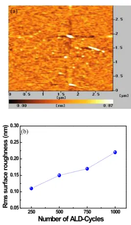
Fig. 4. (a) Surface image of TiO

2

thin films measured by AFM (1,000 ALD-cycles TiO

2

), and (b), the change of rms surface roughness of TiO

2

films as a function of number of ALD-cycles.

그림 3은 원자층 증착장치로 1,000 사이클에서 제작 되어진 TiO

2

박막의 FESEM 표면이미지를 보여준다.

표면에서 확인할 수 있듯이, 어떠한 결함 없이 아주 균일한 형태를 나타내는 것을 확인할 수 있다.

그림 4는 원자층 증착장치로 제작되어진 TiO

2

박막 의 AFM 으로 측정되어진 표면이미지와 root-mean squared (Rms) 표면거칠기의 변화를 나타낸다. 그림 4(a)는 원자층 증착 장치로 1,000 ALD 사이클에서 제 작된 TiO

2

박막의 AFM 표면 이미지를 보여준다. 결과 에서 보듯이 표면 특성은 균일하고 매우 부드러운 표 면을 가진다. 또한 그림 4(b)이 결과에서 확인할 수 있 듯이 ALD 사이클의 수가 증가할수록 Rms 표면 거칠 기 값은 0.11 nm에서 0.22 nm의 값으로 증가하였다.

이러한 결과는, ALD 사이클 수가 증가할수록 전구체

의 온도는 높아지게 되고, 전구체의 온도가 높을수록

반응성이 증가하여 증착률이 증가한다. 다시 말해,

(4)

(a)

250 500 750 1000

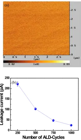
0 50 100 150 200 250

Number of ALD-Cycles

L e a k a g e c u rr e n t (p A ) (b)

Fig. 5. (a) Surface leakage current of TiO

2

thin films measured by AFM (1,000 ALD-cycles TiO

2

), and (b), the change of surface leakage current of TiO

2

films as a function of number of ALD-cycles.

ALD-사이클 주기가 증가하게 되면 TTIP의 자체 분해 온도가 증가하게 되어 확산 반응이 증가하게 되고 이 는 박막 성장 시 표면온도를 상승시키고, 박막의 표면 결정화를 향상시키는 역할을 한다 [12-14]. 이러한 결 과는 ALD 사이클의 수 증가는 TiO

2

박막의 두께와 표 면의 결정화에 기여한다고 판단할 수 있다.

그림 5(a)는 1,000 ALD 사이클에서 제작되어진 TiO

2

박막의 SPM 장치를 이용하여 측정되어진 누설전 류 값을 이미지로 보여주었으며, 그림 5(b)는 ALD 사 이클이 증가에 따른 SPM 장치로 측정되어진 누설전 류의 값의 변화를 보여준다. 그림 5(a)의 결과에서 원자층 증착장치로 제작되어진 TiO

2

박막은 원자단위 로 균일한 표면을 이루고 있으며, 이러한 균일한 표 면에서 측정되어진 표면 누설전류 값은 균일한 값을 나타낸다는 것을 이미지에서 확인할 수 있으며, 그림 5(b)의 결과에서는 ALD 사이클의 수가 증가함에 따 라 표면 누설전류 값은 감소한다는 것을 확인하였다.

Fig. 6. Leakage current of TiO

2

thin films (MIM structure) measured by SPM (1,000 ALD-cycles TiO

2

).

또한, 1,000 ALD 사이클에서는 표면 누설전류 평균 값이 25 pA로 아주 낮은 값을 나타낸다. ALD 사이클 의 수의 증가는 TiO

2

박막의 두께를 증가시키며, 또한 박막의 표면 결정화를 진행시켜, 결과적으로 박막의 절 연 특성 향상을 의미한다. 결론적으로 ALD 사이클의 수의 증가는 TiO

2

박막의 전기적 절연 특성을 증가시 킨다.

그림 6은 1,000 ALD 사이클에서 제작되어진 TiO

2

박막을 절연체 층으로 금속-절연체-금속(metal-insulator-metal) 구 조를 제작하여 측정한 누설전류값을 나타낸다. 그림에 서는 박막의 여러 부분에서 측정되어진 누설전류 값의 변화를 보여주고 있으며 누설전류값이 19 pA에서 30 pA 사이의 값의 변화를 나타내었다. 금속-절연체-금속 구조에서도 거의 모든 부분에서 유사한 누설전류값을 가진다는 것을 확인할 수 있으며, SPM 장치로 측정 되어진 표면 누설전류값의 특성 결과와 거의 일치하는 것을 확인하였다 [15,16]. 결과로서 ALD 사이클의 수 의 증가는 TiO

2

박막의 절연 특성을 향상시킨다.

4. 결 론

폴리머 절연체 코팅 응용을 위하여 원자층 증착 장 치로 폴리머 절연체와 실리콘 기판 위에 TiO

2

박막을 합성하였으며, ALD 사이클의 수에 따라 제작된 TiO

2

박막의 표면 및 전기적 특성을 고찰하였다. 본 실험에

사용되어지는 폴리머 절연체는 90

o

이상의 접촉각을

가지는 발수 특성을 나타내는데, 이 기판 위에 ALD

사이클의 수를 증가시켜 TiO

2

박막을 폴리머 절연체

기판위에 합성하였으며, ALD 사이클 수가 증가함에

따라 TiO

2

박막의 표면의 접촉각 값은 증가하여 초발

(5)

이 표면에서는 균일한 누설전류 값을 나타내었으며, ALD 사이클의 수가 증가함에 따라 표면 누설전류 값 은 감소하였으며, 1,000 ALD 사이클에서 25 pA의 아주 낮은 표면 누설전류 값을 나타내었다.

REFERENCES

[1] J. M. Kim, T. W. Nam, S. J. Lim, Y. G. Seol, N. E.

Lee, D. Y. Kim, and H. Kim, Appl. Phys. Lett., 98, 142113 (2011). [DOI: http://dx.doi.org/10.1063/1.3577607]

[2] E. Guziewicz, I. A. Kowalik, M. Godlewski, K. Kopalko, V. Osinniy, A. Wojcik, S. Yatsunenko, E. Usakowska, W.

Paszkowicz, and M. Guziewicz, J. Appl. Phys., 103, 033515 (2008). [DOI: http://dx.doi.org/10.1063/1.2836819]

[3] J. Sheng, N. Yoshida, J. Karasawa, and T. Fukami, Sens.

Actuators B, 41, 131 (1997).

[DOI: http://dx.doi.org/10.1016/S0925-4005(97)80285-7]

[4] J. K. Luo, Y. Q. Fu, H. R. Le, J A. Williams, S. M.

Spearing, and W. I. Milne, J. Micromech. Microeng., 17, S147 (2007). [DOI: http://dx.doi.org/10.1088/0960-1317/17/7/S12]

[5] D. Sheeja, B. K. Tay, S. P. Lau, and X. Shi, Wear, 249, 433 (2001). [DOI: http://dx.doi.org/10.1016/S0043-1648(01)00541-5]

[6] M. Schlatter, Diam. Relat. Mater., 11, 1781 (2002).

[DOI: http://dx.doi.org/10.1016/S0925-9635(02)00166-8]

[DOI: http://dx.doi.org/10.1016/0040-6090(92)90874-B]

[10] W. R. Hansen and K. Autumn, Proc. Natl. Acad. Sci.

USA, 102, 385 (2005).

[DOI: http://dx.doi.org/10.1073/pnas.0408304102]

[11] M. Ma and R. M. Hill, Curr. Opin. Colloid Interface Sci., 11, 193 (2006).

[DOI: http://dx.doi.org/10.1016/j.cocis.2006.06.002]

[12] M. Heikkila, E. Puukilainen, M. Ritala, M. Leskela, Journal of Photochemistry and Photobiology A: Chemistry, 204, 200 (2009).

[DOI: http://dx.doi.org/10.1016/j.jphotochem.2009.03.019]

[13] A. Fujishima, X. Zhang, and D. A. Tryk, Surface Science Reports, 63, 515 (2008).

[DOI: http://dx.doi.org/10.1016/j.surfrep.2008.10.001]

[14] G. J. Choi, S. K. Kim, S. J. Won, H. J. Kim, and C. S.

Hwang, Journal of The Electrochemical Society, 156, G138-G143 (2009).

[DOI: http://dx.doi.org/10.1149/1.3169516]

[15] S. K. Kim, W. D. Kim, K. M. Kim, C. S. Hwang, and J. Jeong, Appl. Phys. Lett., 85, 4112 (2004).

[DOI: http://dx.doi.org/10.1063/1.1812832]

[16] S. K. Kim, G. W. Hwang, W. D. Kim, and C. S.

Hwang, Electrochem. Solid-State Lett., 9, F5 (2006).

[DOI: http://dx.doi.org/10.1149/1.2131241]

수치

Fig.  1.  Contact  angle  shapes  of  TiO 2   thin  films  synthesized  on  polymer  insulator  with  various  number  of  ALD-cycles;  (a)  250,  (b)  500,  (c)  750,  and  (d)  1,000  cycles
Fig.  3.  FESEM  surface  images  of  TiO 2   film  synthesized  on  silicon  substrate  at  the  condition  of  1,000  cycles  ALD-cycles.
Fig.  6.  Leakage  current  of  TiO 2   thin  films  (MIM  structure)  measured  by  SPM  (1,000  ALD-cycles  TiO 2 ).

참조

관련 문서

This is an Open-Access article distributed under the terms of the Creative Commons Attribution Non-Commercial License (http://creative- commons.org/licenses/by-nc/3.0)

This is an Open-Access article distributed under the terms of the Creative Commons Attribution Non-Commercial License

This is an Open-Access article distributed under the terms of the Creative Commons Attribution Non-Commercial License

This is an Open-Access article distributed under the terms of the Creative Commons Attribution Non-Commercial License

This is an Open-Access article distributed under the terms of the Creative Commons Attribution Non-Commercial License

This is an Open-Access article distributed under the terms of the Creative Commons Attribution Non-Commercial License

This is an Open-Access article distributed under the terms of the Creative Commons Attribution Non-Commercial License

This is an Open-Access article distributed under the terms of the Creative Commons Attribution Non-Commercial License