Vol. 26, No. 8 (2016)
430
Atomic Layer Deposition of Al
2O
3Thin Films Using Dimethyl Aluminum sec-Butoxide and H
2O Molecules
Byeonghyeon Jang and Soo-Hyun Kim
†School of Materials Science and Engineering, Yeungnam University, Gyeongsan-si 38541, Republic of Korea (Received June 22, 2016 : Revised June 22, 2016 : Accepted July 8, 2016)
Abstract
Aluminum oxide (Al2O3) thin films were grown by atomic layer deposition (ALD) using a new Al metalorganic precursor, dimethyl aluminum sec-butoxide (C12H30Al2O2), and water vapor (H2O) as the reactant at deposition temperatures ranging from 150 to 300oC. The ALD process showed typical self-limited film growth with precursor and reactant pulsing time at 250oC; the growth rate was 0.095 nm/cycle, with no incubation cycle. This is relatively lower and more controllable than the growth rate in the typical ALD-Al2O3 process, which uses trimethyl aluminum (TMA) and shows a growth rate of 0.11 nm/cycle. The as-deposited ALD-Al2O3 film was amorphous; X-ray diffraction and transmission electron microscopy confirmed that its amorphous state was maintained even after annealing at 1000oC. The refractive index of the ALD-Al2O3 films ranged from 1.45 to 1.67; these values were dependent on the deposition temperature. X-ray photoelectron spectroscopy showed that the ALD-Al2O3 films deposited at 250oC were stoichiometric, with no carbon impurity. The step coverage of the ALD-Al2O3 film was perfect, at approximately 100 %, at the dual trench structure, with an aspect ratio of approximately 6.3 (top opening size of 40 nm). With capacitance-voltage measurements of the Al/ALD-Al2O3/p-Si structure, the dielectric constant of the ALD- Al2O3 films deposited at 250oC was determined to be ~8.1, with a leakage current density on the order of 10−8A/cm2 at 1 V.
Key words
aluminium oxide, atomic layer deposition, dimethyl aluminum sec-butoxide, trimethyl aluminum, growth rate.1. Introduction
With the continuous scaling down of Si-based semi- conductor devices, many materials have been identified as high-permittivity(high- k) materials with a higher die- lectric constant than SiO
2for their better performance and greater functionality.
1-2)Important concerns on them include the interface quality,
2-3)film morphology,
4-5)and reliability. Among them, aluminum oxide (Al
2O
3) thin films
3,6-10)have been studied extensively and applied to commercial logic devices
11)and dynamic random access memory(DRAM)
12)as a gate oxide or capacitor dielectric owing to its excellent properties, such as high band gap (8~9 eV) leading to a low leakage current, high thermal stability to maintain an amorphous structure up to 1000
o
C annealing, good interface with Si, resulting in a low defect density (< 10
11cm
−2), and a high negative fixed charge density (> 10
12cm
−2).
13-15)Apart from its main appli- cations for semiconductor devices mentioned above, Al
2O
3thin films are commonly used as a protective layer
and ion barrier for photovoltaic cells and gas diffusion barriers for organic displays.
16-18)All these applications require the Al
2O
3films to have good homogeneity, low surface roughness, and good control of the film thickness for films in the order of 10 Å or less. A range of de- position techniques, such as sputtering,
19)chemical vapor deposition,
15,20)pulsed laser deposition,
21)and thermal evaporation
22)have been introduced for preparing the Al
2O
3thin films. On the other hand, these methods have an inherent limitation to be applied for potential higher performance devices with very complex, small sized, and high aspect ratio structures. Atomic layer deposition (ALD) can provide a viable solution for the deposition of Al
2O
3thin films for those emerging applications because ALD can provide excellent conformality, digital controlla- bility of the film thickness, and large-area uniformity owing to its inherent surface-saturated and self-limited reaction mechanisms.
23)Many Al precursors have been identified for successful ALD-Al
2O
3processes
24-29)but alkyl aluminum or alkyl
†Corresponding author
E-Mail : [email protected] (S.-H. Kim, Yeungnam Univ.)
©Materials Research Society of Korea, All rights reserved.
This is an Open-Access article distributed under the terms of the Creative Commons Attribution Non-Commercial License (http://creative- commons.org/licenses/by-nc/3.0) which permits unrestricted non-commercial use, distribution, and reproduction in any medium, provided the original work is properly cited.
aluminum hydride is typically used for commercial ALD- Al
2O
3processes
30-33)because they have high vapor pre- ssures [e.g., in the case of trimethyl aluminum(TMA), 9 torr at 20
oC] to guarantee a reliable supply of the pre- cursor into the deposition chamber, relatively inexpensive, very reactive with typical oxidants, such as H
2O, O
2, and O
3, and relatively low temperature growth is possible. In the growth process using a liquid source of TMA and H
2O, it is unnecessary to recharge the source materials for every run, which is in contrast to the process using solid source, such as AlCl
3. One of the disadvantages of alkyl aluminum precursors, such as TMA is that they are pyrophoric, which requires special handling and storage precautions.
8)In addition, ultra-thin thickness control is difficult in the ALD-Al
2O
3process using TMA because of the relatively rapid growth rate.
34)In addition, the TMA precursor in ALD has a disadvantage of the incorporation of impurities, C and H, during film growth via a reaction between the precursor and reactant. Incorporated H was reported to increase the leakage current of the dielectric layer
35)and the as-deposited Al
2O
3films showed a very large leakage current compared to those of post-annealed films.
36)To address these problems with ALD-Al
2O
3pro- cesses, other Al metalorganic precursors, such as aluminum isopropoxide (C
9H
21AlO
3), have been used. On the other hand, this compound polymerizes easily and exists as a mixture of polymers or oligomers.
37)Each polymer or oligomer has a different vapor pressure. As a result, the vapor pressure of this precursor is unpredictable and diffi- cult to control. Aluminum 2-ethylhexanoate (C
16H
31AlO
5) has also been used as a precursor for the ALD-Al
2O
3process, but its low vapor pressure results in a low de- position rate, which limits its use.
In this study, Al
2O
3thin films were deposited by ALD using new non-pyrophoric Al precursor, dimethyl alumi- num sec-butoxide (DMASBO, C
12H
30Al
2O
2), which is even stable in air and the vapor pressure is sufficiently high to be applied to ALD with H
2O as a reactant. The growth kinetics at deposition temperatures ranging from 150 to 300
oC was investigated and compared with that of the TMA-based ALD-Al
2O
3process. In addition, film properties, such as the phase, density, refractive index, composition, step coverage, and thermal stability were characterized using a range of analysis tools. Finally, ALD-Al
2O
3films were evaluted as a capacitor dielectric.
2. Experimental Procedure
Al
2O
3thin films were deposited in a travelling-wave type ALD reactor (Lucida-D100, NCD technology) using a new Al metalorganic precursor, (dimethyl aluminum sec-butoxide) (C
12H
30Al
2O
2) and water vapor as the react- ant. The new Al metalorganic precursor is liquid at room
temperature and has a vapor pressure of 0.9 Torr at 63
oC. Fig. 1 shows the molecular structure of the Al precursor used in this study. The deposition temperatures ranging from 150 and 300
oC were varied to find a possible ALD temperature window of the present ALD scheme whereas the typical deposition temperature was 250
oC. P-type Si (100) wafers covered with 100-nm- thick thermally grown SiO
2were used as the substrates.
The chamber was evacuated to ~ 0.05 Torr prior to de- position and the chamber pressure was approximately 0.5 Torr during deposition. The precursor was heated to 56
oC to reliably provide the precursor to the chamber and the temperature of the precursor delivery line was maintained at 100
oC to prevent condensation of the Al precursor during delivery. Water vapor, which was carried by 100 sccm of N
2gas, was also provided to the chamber as a reactant. Between the precursor and react- ant pulsing steps, a purging process was performed with 200 sccm of N
2; each ALD cycle involved precursor pulsing, purging, reactant pulsing, and purging. From preliminary investigations, basic pulsing conditions were set as follows: precursor pulsing for 3 s, reactant pulsing for 1 s, and purging for 10 s. Such a condition was sufficient to guarantee self-limited growth of the ALD- Al
2O
3films.
The thickness and density of the Al
2O
3films were
determined by X-ray reflectance (XRR, PANalytical X’-
pert MRD with Cu-K
αradiation at 1.5 kW). For phase
identification, grazing-incidence angle (incident angle,
θ = 3
o) X-ray diffraction (GIAXRD, PANalytical X’-pert
MRD with Cu-K
αradiation at 1.5 kW) analysis was
performed. The refractive indices of the films were mea-
sured by spectroscopic ellipsometry. The composition
and chemical bonding within the Al
2O
3films were
analyzed by X-ray photoelectron spectroscopy (XPS, K-
Alpha XPS Spectrometer with monochromated AI Ka in
Fig. 1. The molecular structure of the Al precursor used in this study.Yeungnam University). Plan view transmission electron microscopy (Tecnai F20 equipped with 200 kV accelerating voltage and field emission gun) was used to examine the microstructures of the ALD-Al
2O
3films. The step cover- ages of the films was evaluated on dual trench structures with an aspect ratio(AR) of ~6.3(bottom width: 15 nm) using cross-sectional view transmission electron micros- copy(XTEM). The electrical properties, such as capacitance and leakage current of the fabricated MOS capacitor sample were measured using a probe station(Keithley 306 electrometer).
3. Results and Discussion
3.1 Growth kinetics of ALD-Al
2O
3process
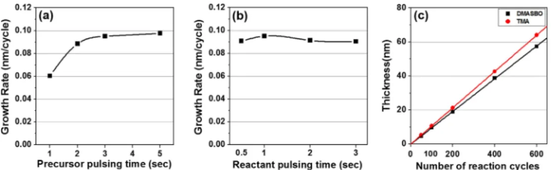
The growth kinetics of the ALD-Al
2O
3process was examined at a deposition temperature of 250
oC. Fig. 2(a) shows the growth rates of the films as a function of the precursor pulsing time at a fixed reactant pulsing time of 1 s. The growth rates were determined by dividing the measured film thicknesses by the number of ALD re- action cycles. With increasing precursor pulsing time from 1 s to 3 s, the growth rate was increased; the grow rate was changed slightly by further increasing the precursor pulsing time to 5 s. The growth kinetics was also investigated according to the reactant pulsing time at a fixed precursor pulse time of 3 s(Fig. 2(b)). The results showed a constant growth rate at a very short pulse of H
2O longer than 0.5 s. These results clearly show that self-limited growth behavior of the ALD-Al
2O
3films occurred using the new Al metalorganic precursor and H
2O. Fig. 2(c) shows the thicknesses of the ALD-Al
2O
3films deposited using the basic pulsing conditions as a function of the number of ALD reaction cycles at 250
o
C. For comparison, the results obtained using TMA and water vapor at the same deposition temperature are also shown. For both processes, the Al
2O
3film thicknesses were increased linearly with increasing number of ALD
reaction cycles, which is a typical characteristic of ALD process, and the extrapolated lines clearly showed that no incubation cycles were required for ALD-Al
2O
3film growth. On the other hand, the growth rate of the DMASBO-based ALD-Al
2O
3process was slightly lower (0.095 nm/cycle) than that of the TMA-based ALD-Al
2O
3process (0.125 nn/cycle). Indeed, many reports on the ALD-Al
2O
3process using TMA and H
2O vapor showed growth rates ranging from 0.1 nm/cycle to 0.13 nm/
cycle,
5,9,24,38,39)which were higher than that from the present new Al precursor.
Fig. 3 shows the growth rates of both ALD-Al
2O
3processes obtained under the basic pulsing condition as a function of the deposition temperature. The deposition
Fig. 2. Growth rate of ALD-Al2O3 films deposited on SiO2 substrates after 200 cycles as a function of (a) the Al precursor pulsing time and (b) reactant (H2O molecule) pulsing time. (c) Thickness of the ALD-Al2O3 films deposited on SiO2 substrates as a function of the number of reaction cycles for different ALD-Al2O3 processes. The films were deposited at 250oC under the basic pulsing conditions. The line indicates the linearly fitted line for the thickness data. The thicknesses were measured by X-ray reflectance (XRR) analysis.
Fig. 3. Growth rates of the ALD-Al2O3 films as a function of the deposition temperature from 150 and 300oC. The basic pulsing conditions that guaranteed self-limited film growth were used (precursor pulsing of 3 s, reactant pulsing of 1 s, and precursor and reactant purging of 10 s).
temperature was varied from 150 to 300
oC. The growth rate of the TMA-based ALD-Al
2O
3process was relatively constant, ~0.125 nm/cycle, irrespective of the deposition temperature. On the other hand, the growth rate of the DMASBO-based ALD-Al
2O
3process was dependent on the deposition temperature and generally increased with increasing deposition temperature. At a deposition tem- perature of 150
oC, the growth rate of the DMASBO- based ALD-Al
2O
3process was 0.078 nm/cycle, which is
~38 % lower than that of the TMA-based one. The growth rate was relatively constant, ~0.095 nm/cycle at deposition temperatures ranging from 200 and 275
oC, which is called the ALD temperature window. Above the ALD temperature window, the grow rate again increased to 0.102 nm/cycle but it was still lower than that of the TMA-based one. This indicates that the DMASBO-based ALD-Al
2O
3process has greater potential than the TMA- based ALD-Al
2O
3process in view of the process con- trollability, particularly for very thin films.
3.2 Properties of ALD-Al
2O
3film
The ALD-Al
2O
3films deposited under the basic con- ditions(at 250
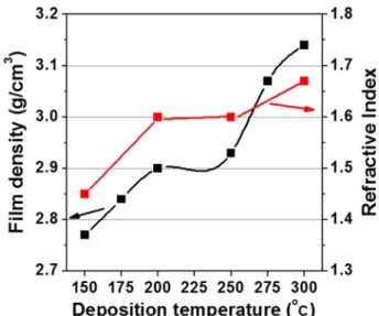
oC within ALD temperature window) were analyzed using a range of techniques. Fig. 4 shows the refractive index and film density of the DMASBO-based ALD-Al
2O
3films as a function of the deposition tem- perature from 150 to 300
oC, which were characterized by ellipsometry and X-ray reflectance analysis(XRR), respectively. The film density of the ALD-Al
2O
3film increased from 2.77 to 3.14 g/cm
3with increasing de- position temperature from 150
oto 300
oC, which is a similar result to that of the TMA-based ALD-Al
2O
3films.
9,14)For example, Oili et al . reported similar results in that the film density increased almost linearly with increasing ALD temperature from 2.85 to 3.10 g/cm
3for the films grown at 110 to 300
oC.
40)The refractive index of the ALD-Al
2O
3films also increased from 1.45 to 1.67 with increasing deposition temperature from 150 to 300
oC and showed a relatively constant value of ~1.6 for the films deposited within the ALD temperature window.
The relationship between the film density and refractive
index can be calculated from the Gladstone-Dale equation (1) or the Lorentz-Lorenz equation (2), where ρ is the density, n is the refractive index, and K
1and K
2are constants. This means the refractive index is related to the film density, as shown in Fig. 3.
14,24)ρ = K
1( n − 1) Eq. (1)
ρ = K
2( n
2− 1) / (n
2+ 2) Eq. (2)
The films deposited under the basic pulsing conditions at 250
oC were analyzed further by XPS to identify the chemical bonding configurations. A survey spectrum acquired at the film surface in the binding energy range of 0~1204 eV(not shown here) showed signals of C(due to surface carbon contamination) as well as Al and O.
Therefore, the XPS data were obtained after sputtering an approximately 4-nm-thick film to remove surface con- tamination and to characterize the bonding status of the film itself. As shown in Fig. 5(a), the C 1s peak, which is generally shown at ~285 eV, was not detected, indi- cating that the film does not contain C. Fig. 5(b) showed
Fig. 4. Refractive index and film density as a function of the deposition temperature from 150 and 300oC.Fig. 5. XPS spectra of the ALD-Al2O3 film deposited at 250oC with the basic pulsing conditions (3s-10s-1s-10s); (a) C 1s (b) Al 2p, (c) O 1s at after etching.
the binding energy of the Al 2p photoelectron and the XPS data were calibrated to the adventitious C 1s peak detected on the film surface. An intensive single peak at 74.5 eV was observed and attributed to Al-O bonding.
The absence of a shoulder peak around 72.5 eV indicates that there were no Al-Al bonds in the film.
3,41)This is probably due to the completely oxidized aluminum by the self-limited surface reaction during the ALD process.
In the case of the O 1s XP spectrum, only a single peak centered at ~530.8 eV was observed, which was assigned to Al-O bonding in the Al
2O
3(Fig. 5(c)). Therefore, XPS analysis strongly supports that the films deposited using a new Al metalorganic precursor, DMASBO, consisted mostly of an Al
2O
3phase.
Fig. 6 shows the XPS depth profile of the Al
2O
3film deposited on a SiO
2substrate. After sputtering an approximately 2-nm-thick film to remove surface con- tamination, the composition of each element was uniform throughout the film thickness. From the aforementioned result, incorporation of carbon impurity was negligible
(less than 0.1 at.%) within the film, indicating that a high-purity Al
2O
3film was deposited. The aluminum to oxygen ratio was quite stoichiometric, 2:3, corresponding to the Al
2O
3composition. Therefore, this indicates that a very pure and quite stoichiometric ALD-Al
2O
3film was deposited using the DMASBO precursor and H
2O as a reactant.
Fig. 7(a) shows the the grazing incident angle (incidence angle = 3º) XRD analysis result of the ALD- Al
2O
3film deposited under the basic pulsing conditions at 250
oC. The grazing-angle XRD is more sensitive for characterizing the crystallinity and phase of ultrathin and nanocrystalline films. Even with sensitive grazing-angle XRD analysis, the result does not show any specific crystalline peaks related to crystalline Al
2O
3and the intensive peak from single crystal Si was only observed at 56
o. This suggests that the ALD-Al
2O
3film forms an amorphous phase, which is similar to that in other deposition systems, such as sputtering, pulsed laser de- position, and chemical vapor deposition.
42-43)The results of the ALD-Al
2O
3prepared using other Al metalorganic precursor also showed the formation of an as-deposited amorphous phase. The plan-view TEM image of the ALD-Al
2O
3(~20 nm-thick) (Fig. 7(b)) shows the micro- structure of the film more obviously. This appears to be featureless, which is typical in an amorphous structure.
The corresponding selected-area electron diffraction analysis [inset of Fig. 7(b)] showed a halo pattern and confirmed that the film was amorphous.
The thermal stability of the ALD-grown Al
2O
3films was examined by annealing the films at high tem- peratures because one of the main applications of ALD- Al
2O
3in this study is its use as a capacitor dielectric in DRAM devices. For example, during DRAM fabrication, the film may experience several high temperature pro- cesses after deposition and possible crystallization may often lead to a modification of the functional properties, such as an increase in leakage current in a DRAM capacitor. Fig. 7(c) shows the grazing incident angle XRD results of the films annealed at various temperatures. No remarkable changes in the XRD results were shown,
Fig. 7. (a) Grazing-angle XRD analysis results (b) plan-view TEM image of ALD-Al2O3 films deposited with basic pulsing condition at 250
oC. (c) grazing-angle XRD pattern (d) the plan view TEM image of ALD-Al2O3 film annealed at the annealing temperature.
Fig. 6. XPS depth profile of ALD-Al2O3 films grown on SiO2 substrates.
even after annealing up to 1000
oC compared to that of the as-deposited film shown at Fig. 7(a). A plan-view TEM image of ALD-Al
2O
3film annealed at 1000
oC(Fig.
7(d)) still appeared to be featureless, which is the same as that of as-deposited film shown at Fig. 7(b). The corresponding selected-area electron diffraction analysis [inset of Fig. 7(d)] showed a halo pattern and confirmed that the film is amorphous. Jakschik et al. reported that an ALD-Al
2O
3film deposited using TMA and H
2O as a reactant remains amorphous up to 900
oC and crystalli- zation proceeded at temperatures above 900
oC.
44)In addition, an ALD-Al
2O
3film deposited using TMA and O
2plasma as a reactant crystallized with a mass loss of
~5 % and a densification of ~20 % after annealing above 800
oC.
14)Therefore, the present results indicate that
ALD-Al
2O
3film developed in this study has better thermal stability than the ALD-Al
2O
3film deposited using TMA.
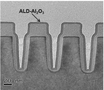
The conformality of the new ALD-Al
2O
3process was evaluated by depositing the film onto the overall nano- scale dual trench structure (top and bottom width: 40 and 15 nm, respectively) with an aspect ratio of ~6.3. The XTEM image(Fig. 8) clearly shows that the ALD-Al
2O
3film was deposited conformally and uniformly on to the surface of the nano-scale dual trench indicating that the step coverage of the ALD-Al
2O
3film was perfect at approximately 100 %. This perfect step coverage indicated that the Al
2O
3film had been deposited under an ideal ALD growth process without partial decomposition of the DMASBO precursors.
Finally, to examine the electrical properties of the DMASBO-based ALD-Al
2O
3films, the MOS capacitor structure sample (Al/Al
2O
3/p-Si) was fabricated with the Al
2O
3film (32 nm in thickness) deposited at 250
oC. The capacitor area was 3.85 × 10
−3cm
2, which was defined by sputtering using a shadow mask during Al metal electrode (100 nm in thickness) deposition. Fig. 9(a) shows the capacitance-voltage results of the ALD-Al
2O
3film using DMASBO, as measured at 100 KHz. The gate voltage was swept from the accumulation region ( −5.0 V) to the inversion region (5.0 V) and back. This shows the typical features of a n-type metal oxide semiconductor (n-MOS) capacitor with an accumulation region at negative biases and an inversion region at positive biases.
These small hysteresis loops are believed to be due to the low impurity content in the film.
41)The maximum ac- cumulation capacitance of the ALD-Al
2O
3using the DMASBO precursor was 810 pF at a gate bias of −5.0 V.
The measured capacitance is similar to the serial capa- citance of the grown ALD-Al
2O
3and adventitious native SiO
2layer. Considering the measured 2 nm thickness the
Fig. 8. Cross-section TEM image of the ALD-Al2O3 film depositedon the dual trench structures with a bottom width of ~15 nm and an AR of 6.3, showing the step coverage of the process.
Fig. 9. (a) Capacitance-voltage characteristics of the Al2O3 film deposited at 250oC from Al/ALD-Al2O3/p-Si capacitor. The data were recorded from accumulation to inversion, and back to accumulation. (b) Current density-voltage characteristics of the Al2O3 film deposited at 250oC from an Al/ALD-Al2O3/p-Si capacitor.
native SiO
2layer, the dielectric constant was calculated from the C-V data of Fig. 9(a). The estimated dielectric constant of the ALD-Al
2O
3using the DMASBO pre- cursor was 8.1. As expected, the dielectric constants of the ALD-Al
2O
3film were lower than that of bulk α- Al
2O
3(~9), due to the lower density, as mentioned above.
Fig. 9(b) shows the I-V characteristics of the ALD-Al
2O
3film with the Al/ALD-Al
2O
3(32 nm in thickness)/p-Si capacitor structure. The leakage current density of the Al
2O
3film using the DMASBO precursor was in the order of ~10
−8A/cm
2. The leakage current value was either similar to or slightly higher than that of the TMA-based ALD-Al
2O
3studies and indicates that the DMASBO- based ALD-Al
2O
3process is not inferior to the electrical properties, such as dielectric constant and leakage current, compared to that of the TMA-based ALD-Al
2O
3process.
6-9)4. Summary and Conclusions
In this study, Al
2O
3films were deposited on thermally grown SiO
2substrates by ALD with the sequential supply of a new Al metalorganic precursor, dimethyl aluminum sec-butoxide (C
12H
30Al
2O
2), and water vapor (H
2O) at deposition temperatures ranging from 150 to 300
oC. The typical ALD characteristics, such as self- limited film growth behavior and linear film growth with the number of ALD reaction cycles, were observed at a deposition temperature of 250
oC. In addition, the growth rate was constant (~0.095 nm/cycle) within the ALD temperature window between 200 and 250
oC with no incubation cycles. The growth rate of the DMASBO- based ALD-Al
2O
3process was relatively low and more controllable between 0.078 nm/cycle and 0.102 nm/cycle depending on the deposition temperature, whereas that of the TMA-based ALD-Al
2O
3process generally showed a growth rate of ~0.125 nm/cycle, independent of the de- position temperature. The properties of the DMASBO- based ALD-Al
2O
3thin films deposited at 250
oC were not inferior to those of the TMA-based ALD-Al
2O
3. The refractive index of the Al
2O
3film varied from 1.45 to 1.67 depending on the deposition temperature. XPS indicated the formation of stoichiometric Al
2O
3with no carbon impurity. The step coverage of the ALD-Al
2O
3film was perfect, approximately 100 %, onto the overall nano-scale dual trench structure(top and bottom width:
40 and 15 nm) with an aspect ratio of ~6.3. The ALD- Al
2O
3film has excellent thermal stability up to 1000
oC by XRD and plan-view TEM analysis. The MOS capacitor of the sputtered-Al/ALD-Al
2O
3/p-Si showed excellent performance with the ALD-Al
2O
3film showing a dielectric constant of 8.1. The leakage current was in the order of 10
−8A/cm
2.
Acknowledgements
This study(2015R1A2A2A04004945) was supported by Mid-career Researcher Program through NRF grant funded by the MEST and also Human Resources Program in the Transportation Specialized Lighting Core Technology Development(No. N0001364) granted financial resource from the Ministry of Trade, Industry & Energy, Republic of Korea. The precursor used in this study was provided by Hansol Chemical Ltd.
References
1. L. Niinisto, J. Paivasaari, J. Niinisto, M. Putkonen and M.
Nieminen, Phys. Status Solidi A, 201, 1443 (2004).
2. L. G. Gosset, J.-F. Damlencourt, O. Renault, D. Rouchon, Ph. Holliger, A. Ermolieff, I. Trimaille, J.-J. Ganem, F.
Martin and M.-N. Semeria, J. Non-Cryst. Solids., 303, 17 (2002).
3. R. Katamreddy, R. Inman, G. Jursich, A. Soulet and C.
Takoudis, J. Electrochem. Soc., 153, C701 (2006).
4. D. M. Hausmann and R. G. Gordon, J. Cryst. Growth, 249, 251 (2003).
5. A. Philip and K. Rajeev Kumar, Ph. D. Thesis, p101- 128, Cochin University of Science and Technology India, (2012).
6. M. D. Groner, J. W. Elam, F. H. Fabregutte and S. M.
George, Thin Solid Films., 413, 186 (2002).
7. K. Kukli, M. Ritala and M. Leskela, J. Vac. Sci. Technol.
A., 15, 2214 (1997).
8. J. Koo, S. Kim, S. Jeon and H. Jeon, J. Korean Phys.
Soc., 48, 131 (2006).
9. M. D. Groner, J. W. Elam, F. H. Fabregutte and S. M.
George, Chem. Mater., 16, 639 (2004).
10. J. L. Hemmen, S. B. S. Heil, J. H. Klootwijk, F.
Roozeboom, C. J. Hodson, M. C. M. Snaden and W. M.
M. Kessels, J. Electrochem. Soc., 154, G165 (2007).
11. F. Campabadal, J. M. Rafi, M. Zabala, O. Beldarrain, A.
Faigon, H. Castan, A. Gomez, H. Garcia and S. Duenas, J. Vac. Sci. Technol. B, 29, 01AA07 (2011).
12. E. Gerritsen, N. Emonet, C. Caillat, N. Jourdan, M.
Piazza, D. Fraboulet, B. Boeck, A. Berthelot, S. Smith and P. Mazoyer, Solid State Electron., 49, 1767 (2005).
13. L. Zhang, H. C. Jiang, C. Liu, J. W. Dong and P. Chow, J. Phys. D: Appl. Phys., 40, 3707 (2007).
14. V. Cimalla, M. Baeumler, L. Kirste, M. Prescher, B.
Christian, T. Passow, F. Benkhelifa, F. Bernhardt, G.
Eichapfel, M. Himmerlich, S. Krischok and J. Pezoldt, Mater. Sci. Appl., 5, 628 (2014).
15. R. S. Johnson, G. Lucovsky and I. Baumvol, J. Vac. Sci.
Technol. A, 19, 1353 (2001).
16. R. Katamreddy, R. Inman, G. Jursich, A. Soulet and C.
Takoudis, Appl. Phys. Lett., 89, 262906 (2006).
17. B. C. O’Regan, S. Scully, A. C. Mayer, E. Palomares and J. Durrant, J. Phys. Chem. B, 109, 4616 (2005).
18. M. D. Groner, S. M. George, R. S. Mclean and P. F.
Carcia, Appl. Phys. Lett., 88, 051907 (2006).
19. R. S. Nowicki, J. Vac. Sci. Technol., 14, 127 (1977).
20. C.-S. Park. J.-G. Kim and J. S. Chun, J. Vac. Sci. Technol.
A, 1, 1820 (1983).
21. J.-P. Barnes, A. K. Petford-Long, R. C. Doole, R. Serna, J. Gonzalo, A. Suarez-Garcia, C. N. Afonso and D. Hole, Nanotechnology, 13, 465 (2002).
22. D. Hoffman and D. Leibowitz, J. Vac. Sci. Technol., 8, 107 (1971).
23. H. Kim, H.-B.-R. Lee and W.-J Maeng, Thin Solid Films, 517, 2563 (2009).
24. A. W. Ott, J. W. Klaus, J. M. Johnson and S. M. George, Thin Solid Films, 292, 135 (1997).
25. M. Ritala, H. Saloniemi, M. Leskelä, T. Prohaska, G.
Friedbacher and M. Grasserbauer, Thin Solid Films, 286, 54 (1996).
26. L. Hiltunen, H. Kattelus, M. Leskelä, M. Mäkelä, L.
Niinistö, E. Nykänen, P. Soininen and M. Tiitta, Mater.
Chem. Phys., 28, 379 (1991).
27. M. Ritala, M. Leskelä, J.-P. Dekker, C. Mutsaers, P. J.
Soininen and J. Skarp, Chem. Vap. Deposition, 5, 7 (1999).
28. V. E. Drozd, A. P. Baraban and I. O. Nikiforova, Appl.
Surf. Sci., 82/83, 583 (1994).
29. E. P. Gusev, M. Copel, E. Cartier, I. J. R. Baumvol, C.
Krug and M. A. Gribelyuk, Appl. Phys. Lett., 76, 176 (2000).
30. R. Matero, A. Rahtu, M. Ritala, M. Leskelä and T.
Sajavaara, Thin Solid Films, 368, 1 (2000).
31. A. W. Ott, K. C. McCarley, J. W. Klaus, J. D. Way and
S. M. George, Appl. Surf. Sci., 107, 128 (1996).
32. G. S. Higashi and C. G. Fleming, Appl. Phys. Lett., 55, 1963 (1989).
33. S. M. George, A. W. Ott and J. W. Klaus, J. Phys. Chem., 100, 13121 (1996).
34. T. Cheon, S.-H. Choi, S.-H. Kim and D.-H. Kang, Electrochem. Solid-State Lett., 14, D57 (2011).
35. T. Aoyama, S. Saida, Y. Okayama, M. Fujisaki, K. Imai and T. Arikade, J. Electrochem. Soc., 143, 977 (1996).
36. P. Ericsson, S. Bengtsson and J. Skarp, Microelectron.
Eng., 36, 91 (1997).
37. J. A. Aboaf, J. Electrochem. Soc., 114, 948 (1967).
38. S. Yun, K. Lee, J. Skarp, H. Kim and K. Nam, J. Vac.
Sci. Technol. A, 12, 2993 (1997).
39. N. D. Hoivik, J. W. Elam, R. J. Linderman, V. M. Bright, S. M. George and Y. C. Lee, Sens. Actuators A Phys., 103, 100 (2003).
40. O. M. E. Ylivaara, X. Liu, L. Kilpi, J. Lyytinen, D.
Schneider, M. Laitinen, J. Julin, S. Ali, S. Sintonen, M.
Berdova, E. Haimi, T. Sajavaara, H. Ronkainen, H.
Lipsanen, J. Kosoinen, S.-P. Hannula and R. L. Puurunen, Thin Solid Films, 552, 124 (2014).
41. S. Kim, S. Lee, C, Hwang, Y. Min, J. Won and J. Jeong, J. Electrochem. Soc., 153, F69 (2006).
42. S. K. Pradhan, P. J. Reucroft and Y. Ko, Surf. Coat.
Technol., 176, 382 (2004).
43. P. katiyar, C. Jin and R. J. Narayan, Acta Mater., 53, 2617 (2005).
44. S. Jakschik, U. Schroeder, T. Hecht, M. Gutsche, H. Seidl and J. W. Bartha, Thin Solid Films, 425, 216 (2003).