1. 서 론
최근 액티브-매트릭스 방식의 디스플레이에 대한 백 플레인 기술로서 비정질의 Si와 다결정질의 Si 기반의 TFT (thin-film transistor)에 대한 잠재적인 대안으 로 산화물 박막 트랜지스터가 큰 주목을 받고 있다.
실리콘 기반의 반도체에 비해서 산화물 반도체는 높은 이동도와 저렴한 가격, 우수한 소자 균일성을 가지고 있으며 대면적화, 고해상도로 발전되어지는 기존과는
a. Corresponding author; [email protected] Copyright ©2017 KIEEME. All rights reserved.
This is an Open-Access article distributed under the terms of the Creative Commons Attribution Non-Commercial License (http://creativecommons.org/licenses/by-nc/3.0) which permits unrestricted non-commercial use, distribution, and reproduction in any medium, provided the original work is properly cited.
다른 최신 디스플레이의 구동소자로 응용할 수 있다는 장점이 있다 [1-3]. 이러한 산화물 반도체는 다양한 물질 로 제작되고 있으며, 이 중에서도 TiOx는 루틸(rutile)과 아나타제(anatase)의 경우 각각 자외선 영역에 속하는 band gap을 가지고 있다. 이러한 넓은 band gap과 저렴한 가격, 그리고 부식과 외부광원과 같은 외부환경 에 대해서 견딜 수 있는 지속성 및 안정적인 상태를 가지며, 높은 굴절률과 적절한 유전율로 인해서 다른 산화물 반도체에 비해 뛰어난 효율을 보이므로 TFT에 서 active layer로 많은 주목을 받고 있다 [4-6]. 그리 고 이러한 TiOx의 두드러지는 장점 중에서 풍부한 자원 량과 효율성 있는 비용은 디스플레이의 구동 소자로서 의 응용을 크게 향상시킬 수 있다 [7,8].
특히 N-type 반도체 특성을 갖는 TiOx TFT는 펄스
원자층 증착 기술을 이용한 TiO
x기반 TFT의 어닐링 효과
김한상1, 김성진1,2,a
1 충북대학교 전자정보대학
2 충북대학교 컴퓨터정보통신연구소
Annealing Effect on TiO
xBased Thin-Film Transistors with Atomic Layer Deposition
Han-Sang Kim
1and Sung-Jin Kim
1,2,a1 College of Electrical and Computer Engineering, Chungbuk National University, Cheongju 28644, Korea
2 Institute for Computer and Information Communication, Chungbuk National University, Cheongju 28644, Korea
(Received February 22, 2017; Revised April 12, 2017; Accepted April 23, 2017)
Abstract: We report on thin-film transistors based on TiOx pre-annealed by femtosecond laser pulses. A 30-nm thick TiOx
active channel layer was initially deposited by an ALD system. The TiOx semiconducting films were annealed by irradiation with a femtosecond laser (power: 3 W/cm2) for 5, 25, and 50s. Atomic force microscopy images revealed that the surface of a TiOx film without femtosecond laser pre-annealing was relatively rough, while after annealing with femtosecond laser pulses, the surface of the TiOx films became smooth. With increasing radiation time, the surrounding gas atmosphere could have a larger impact on the TiOx surface; meanwhile, the thin-film roughness decreased. Thin-film transistors with TiOx active channels pre-annealed at 50s exhibited good transfer characteristics and an on-to-off current ratio of ~103.
Keywords: TiOx, Thin-film transistor, Atomic layer deposition, Annealing
ISSN 1226-7945(Print), 2288-3258(Online)
레이저증착법(pulsed laser deposition) [9], 스프레이 열 분해법(spray pyrolysis), 용액 공정(solution-process) [10,11], 스퍼터(magnetron sputtering) [12-14], 금 속-유기물 화학 기상법(metal-organic chemical vapor deposition) [15]과 같은 여러 방법으로 제작되고 있 다. 그러나 이러한 TiO2 기반의 트랜지스터의 다양한 제작 방법에도 불구하고 현재까지의 전기적 특성은 매 우 낮아 고속 스위칭이 필요한 고성능 디스플레이의 구동 소자로서의 적용에 어려운 점이 있다.
따라서 기존의 방법으로는 낮은 전기적 특성을 갖는 한계점을 보이므로 이러한 한계를 벗어나기 위해서 전 기적 특성을 높이기 위해 TiOx active layer에 대해서 반도체 계면의 막질과 계면에서의 전자 포획을 향상시 키는 ALD (atomic layer deposition) 기술을 사용하였 다. 따라서 ALD 기술로 제작되어진 TiOx active layer 는 넓은 공간에서의 균일성, 원자 수준에서의 정확한 두께 제어 및 낮은 성장 온도와 높은 종횡비(aspect ratio)를 가지므로 뛰어난 저온 증착이 가능해져서 flexible TFT에 적용될 수 있게 된다. 도펀트(dopant) 원자가 이동하는 것을 최소화시키고 전극 저항을 낮추 어 소자의 저항을 낮추는 femtosecond laser pre- annealing을 통해 TiOx 반도체 박막을 만들었고 최적 화한 후 전기적 특성을 평가하였다.
2. 실험 방법
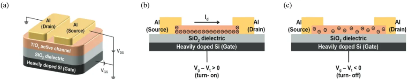
그림 1(a)는 이번 연구에서 비정질 산화물인 TiOx
기반의 TC-BG (top-contact bottom-gate) 구조로 제작한 TiOx 산화물 박막 트랜지스터에 대한 구조를 나타낸다. 게이트 전극 patterning을 진행하지 않고 게이트를 금속화하여 기판의 상부에 위치하도록 하였 고, 일정한 영역을 가진 전극이 아닌 기판 전체에 전 압을 인가함으로써 두께가 100 nm인 heavily doped
n-type 실리콘 웨이퍼를 기판이자 게이트 전극으로 사 용하였다. 이 후 thermal oxidation을 이용하여 100 nm의 SiO2를 절연막으로 형성하였고, 그 후 piranha cleaning과 표준 세정 공정을 통해서 절연막 위의 오 염 물질들을 제거하였다. 두께가 30 nm인 TiO2 박막 을 제작하기 위해서 ALD 공정을 사용하였다. 그림 1(b)와 (c)에서는 n-type TiOx 트랜지스터에서 문턱전 압(Vth)을 극복한 게이트 전극이 인가되면 유효 채널 부분으로 음전하들이 축적되어 트랜지스터가 작동하게 되는 모습을 보여준다. 그리고 트랜지스터가 off 상태 (Vg-Vt > 0)가 되면 채널에서 풀려나는 음전하들로 인 하여 전류의 흐름이 없어지는 모습을 보여주고 있다.
그림 2(a)는 실험에서 사용된 ALD 시스템의 구조도 이다. ALD 공정 시스템은 기본적으로 TiO2의 전구체 인 TDMAT (tetrakis-dimethyl-amino-titanium)와 oxygen의 전구체인 H2O를 반복적으로 증착하여 박 막을 성장시키는 원리다. TDMAT 챔버를 60℃로 가 열한 후에 유체의 양을 조절하는 MFC (mass flow controller)를 통해서 50 sccm의 질소 가스를 챔버로 주입하여 TDMAT 증기를 process chamber로 이동 시켰다. H2O와 TDMAT의 증기가 주입되어지는 과정 이 진행되는 동안에 2.5 × 10⁻² torr의 압력과 200℃
의 온도에서 공정을 진행해서 TiO2를 증착하였다.
그림 2(b)는 ALD의 gas line, source canister, pumping part, hot-trap 부분이 있는 내부 모습을 보여준다. TDMAT는 매우 높은 진공 압력을 갖기 때 문에 부식성이 없는 성장을 보여주고 결과적으로 깨끗 한 막을 생산한다. 그러므로 TDMAT는 ALD 공정 기 술을 사용하는 TiO2 박막의 증착에 가장 적절한 전구 물질이 되어왔다 [16,17].
TiO2 박막을 증착한 후 active layer로 상변이 시키 기 위해서 femtosecond laser pre-annealing과 급속 열처리 기술인 RTA를 600℃의 온도에서 5분 동안 진 행하여 산소가 결핍된 30 nm 두께의 TiOx 층을 제작하 (a)
(b)
(c)
Fig. 1. Schematic representation of (a) the TiOx-TFT structure, (b) turn-on state (Vg-Vt < 0), and (c) turn-off state (Vg-Vt > 0).
였다. 이 후 2,000 µm의 channel length 값과 200 µm 의 channel width 값을 갖는 channel을 생성하였다.
그 후 top-contact 소스(source), 드레인(drain) 전 극을 제작하기 위해 금속 증착기(metal evaporator)를 이용하여 Al을 100 nm 두께로 10-6 torr의 진공도에 서 증착하였다. 최종적으로 반도체 파라미터 측정 장비 인 Agilent 1,500B를 사용하여 소자의 전기적 특성을 상온의 공기 중에서 측정하였고, AFM 장비를 이용하 여 소자의 구조적 성질을 조사하였다.
3. 결과 및 고찰
그림 3은 AFM (atomic force microscope)을 통해 서 femtosecond laser pre-annealing에 의한 표면의 지형 상태를 보여준다. AFM 그림을 보면 femtosecond laser pre-annealing에 대한 열처리 시간이 증가함에 따라 TiOx의 모든 표면들이 핀 홀이 없는 표면과 큰 grain을 성장하는 모습이 관찰되었다. 이것은 TiOx TFT 의 고질적인 전기적인 특성 저하를 개선시키고자 charge
trapping sites들을 제거하고 누설 전류를 개선한 효 과를 예상한다.
그림 4에서는 각각 5s, 25s, 50s에서 femtosecond laser pre-annealing을 사용하여 제조된 TiOx active layer 기반의 박막 트랜지스터에서 VDS가 25 V인 게 이트 전압에 따른 drain 전류에 대한 transfer characteristic curve를 나타낸다. 5s 박막 조사 TFT는 특히 off 전류가 채널에서의 음전하들의 소거가 완전 하지 않아 매우 안정하지 못하며 다소 높은 off 전류 특성을 나타내었다. 반면에 25s, 50s의 femtosecond laser에 의해 형성된 TiOx active layer를 가지는 박 막 트랜지스터는 -10-10 A의 off 전류를 관찰하였다.
표 1을 참고하면 25s, 50s에서의 박막 트랜지스터는 (a)
(b)
Fig. 2. (a) Schematic illustration of ALD system and (b) the interior structure of ALD.
(a) (b)
(c)
Fig. 3. AFM topographies by femtosecond laser pre-annealing at (a) 5s, (b) 25s, and (c) 50s respectively.
-10 0 10 20 30
10-10 10-9 10-8 10-7
Id (A)
Vg (V) 5 s 25 s 50 s
Fig. 4. Transfer characteristics with the drain current versus gate-voltage behavior at VDS of 25 V for the TiOx based TFTs by femtosecond laser pre-annealing at (a) 5s, (b) 25s, and (c) 50s respectively.
특히 off 전류 값이 개선되어 on/off current ratio (Ion/Ioff)가 5s에 비해서 크므로 좋은 전달 특성을 보인 다. 또한 전체적으로 문턱 전압의 positive shift 현상 을 보였지만 pre-annealing 시간이 증가될수록 조금씩 개선됨을 확인할 수 있었다. 이것은 향후에 O2/plasma 또는 self assembly monolayer의 추가 공정을 실 시하여 보완할 예정이다. Mobility도 0.01 cm2/Vs로 5s에 비해서 높은 수치를 보여서 이동도가 빠른 좋은 성 능을 보이는 것을 확인하였다. 따라서 ALD 공정 전의 femtosecond laser의 pre-annealing 방법에 의해 전 기적인 성능이 향상될 수 있음을 전기적인 특성을 통 하여 확인하였고, TiOx 산화물 박막 트랜지스터가 안정 적으로 구동할 수 있는 열처리 시간을 찾을 수 있었다.
4. 결 론
본 논문에서는 femtosecond laser pre-annealing 에 의해서 TiOx 산화물 박막 트랜지스터의 전기적 성능을 최적화하는 과정을 실시하였다. 실험 결과로 TiOx 막의 표면을 AFM으로 분석하였으며, transfer characteristic을 통해 femtosecond laser에 대한 열 처리 시간이 길어짐에 따라서 향상되어지는 것을 알 수 있었다. 특히 25s, 50s에서의 femtosecond laser pre-annealing 과정을 거친 TiOx 산화물 박막 트랜지 스터가 기존보다 우수한 mobility 값, 낮은 S/S 값, 높은 Ion/Ioff ratio 값을 보인다는 것을 발견하였다. 이 러한 결과로부터 저 비용 생산을 유지하면서 전기적인 성능을 더 향상시키는 실용적이고 잠재적인 가치가 있 는 방법을 보였다.
감사의 글
This research was supported by the Human Resources Development of the Korea Institute of
Energy Technology Evaluation and Planning (KETEP) grant funded by the Korea government Ministry of Trade, industry & Energy (No.
20144030200450). This research was also supported by the MSIP (Ministry of Science, ICT and Future Planning), Korea, under the ITRC (Information Technology Research Center) support program (IITP-2017-2015-0-00448) supervised by the IITP (Institute for Information & communications Technology Promotion).
REFERENCES
[1] K. Nomura, H. Ohta, K. Ueda, T. Kamiya, M. Hirano, and H.
Hosono, Science, 300, 1269 (2003). [DOI: https://doi.org/
10.1126/science.1083212]
[2] K. Nomura, H. Ohta, A. Takagi, T. Kamiya, M. Hirano, and H. Hosono, Nature, 432, 488 (2004). [DOI: https://doi.org/
10.1038/nature03090]
[3] C. G. Van de Walle, Phys. Rev. Lett., 85, 1012 (2000). [DOI:
https://doi.org/10.1103/PhysRevLett.85.1012]
[4] P. H. Wöbkenberg, T. Ishwara, J. Nelson, D.D.C. Bradley, S.
A. Haque, and T. D. Anthopoulos, Appl. Phys. Lett., 96, 082116 (2010). [DOI: https://doi.org/10.1063/1.3330944]
[5] S. K. Kim, W. D. Kim, K. M. Kim, C. S. Hwang, and J.
Jeong, Appl. Phys. Lett., 85, 4112 (2004). [DOI: https://doi.
org/10.1063/1.1812832]
[6] B. J. Choi, D. S. Jeong, S. K. Kim, C. Rohde, S. Choi, J. H.
Oh, H. J. Kim, C. S. Hwang, K. Szot, R. Waser, B. Reichenberg, and S. Tiedke, J. Appl. Phys., 98, 033715 (2005). [DOI:
https://doi.org/10.1063/1.2001146]
[7] A. Hayakawa, O. Yoshikawa, T. Fujieda, K. Uehara, and S.
Yoshikawa, Appl. Phys. Lett., 90, 163517 (2007). [DOI:
https://doi.org/10.1063/1.2730746]
[8] C. J. Liu and J. S. Chen, Appl. Phys. Lett., 80, 2678 (2002).
[DOI: https://doi.org/10.1063/1.1468913]
Laser heat
treatment time (s) Mobility (cm2/Vs) Ion/Ioff Vth (V) S/S
(V/decade)
5 0.00 6.6 × 10 12.0 9.8
25 0.01 1.5 × 10³ 11.5 3.8
50 0.01 1.7 × 10³ 10.6 3.8
Table. 1. Electrical performance of the TiOx based TFTs by femtosecond laser pre-annealing at various laser heat treatment time.
[9] M. Katayama, S. Ikesaka, J. Kuwano, Y. Yamamoto, H.
Koinuma, and Y. Matsumoto, Appl. Phys. Lett., 89, 242103 (2006). [DOI: https://doi.org/10.1063/1.2404980]
[10] J. W. Park and S. Yoo, IEEE Electron Device Lett., 29, 724 (2008). [DOI: https://doi.org/10.1109/LED.2008.2000608]
[11] P. C. Yao, J. L. Chiang, and M. C. Lee, Solid State Sci., 28, 47 (2014). [DOI: https://doi.org/10.1016/j.solidstatesciences.
2013.12.011]
[12] K. H. Choi, K. B. Chung, and H. K. Kim, Appl. Phys. Lett., 102, 153511 (2013). [DOI: https://doi.org/10.1063/1.4802717]
[13] N. Zhong, J. J. Cao, H. Shima, and H. Akinaga, IEEE Electron Device Lett., 33, 1009 (2012). [DOI: https://doi.org/10.1109/
LED.2012.2193658]
[14] K. H. Choi and H. K. Kim, Electrochem. Solid-State Lett., 14, H314 (2011). [DOI: https://doi.org/10.1149/1.3589983]
[15] J. W. Park, S. W. Han, N. Jeon, J. Jang, and S. Yoo, IEEE Electron Device Lett., 29, 1319 (2008). [DOI: https://doi.org/
10.1109/LED.2008.2005737]
[16] J. K. Jeong, J. H. Jeong, H. W. Yang, J. S. Park, Y. G. Mo, and H. D. Kim, Appl. Phys. Lett., 91, 113505 (2007). [DOI:
https://doi.org/10.1063/1.2783961]
[17] J. Kong, J. Lee, Y. Jeong, M. Kim, S. O. Kang, and K. Lee, Appl. Phys. Lett., 100, 213305 (2012). [DOI: https://doi.org/
10.1063/1.4722802]