http://dx.doi.org/10.3938/NPSM.67.136
Structural Properties of MgO Films Deposited on Si(100) Substrates by Using a Combined RF Magnetron Sputtering and Sol-Gel Process
Yida Yang · Hong Seung Kim
∗Department of Electronic Material Engineering, Korea Maritime and Ocean University, Busan 49112, Korea
Nak Won Jang
Division of Electrical and Electronics Engineering, Korea Maritime and Ocean University, Busan 49112, Korea
Young Yun
Division of Radio Communication Engineering, Korea Maritime and Ocean University, Busan 49112, Korea (Received 22 June 2016 : revised 24 November 2016 : accepted 1 December 2016)
The structural properties of MgO films deposited on Si(100) substrates by combining RF sput- tering and the sol-gel process were investigated. The films’ orientation properties, thicknesses and the surface morphologies were investigated by using X-ray diffraction (XRD), transmission electron microscopy (TEM) and atomic force microscopy (AFM). X-ray diffraction and surface morphol- ogy showed that the structures of the films varied with annealing temperature. Crystallizations of (111)-preferentially-oriented MgO films deposited on Si(100) substrates with a MgO buffer layer were easily observed after the samples had been annealed at temperatures above 700◦C. However, the structural properties of the MgO films deposited on MgO buffer layers were almost the same, regardless of the existence of the MgO buffer layer.
PACS numbers: 61.66.Fn, 72.80.Ey, 81.40.Ef, 81.15.Cd
Keywords: MgO film, MgO buffer layer, Annealing temperature, RF magnetron sputter, Sol-gel
I. INTRODUCTION
Generally, MgO is rock salt structure which is the most stable form for highly ionic solids and has been the proto- type for experimental and theoretical studies of neutral and polar oxide surface. The structure consists of two interpenetrating fcc lattices of oxygen anions and metal cations in a +2 oxidation state, making these oxides even more ionic than prototypical ionic NaCl. Due to the de- sirable properties of a wide band gap, low dielectric con- stant (k′ = 9065), low optical loss, and a comparatively low refractive index (∼1.7), MgO single crystal is a pop- ular substrate for preparing ferroelectric thin films [1].
More importantly, MgO can grow epitaxially on Si and GaAs at low temperature below 400 ◦C. In addition,
∗E-mail: [email protected]
it can also be grown on some other substrates, such as Al2O3 [2,3], Fe [4], Ag [5,6], Mo [7] and so on.
Currently, there are many methods to prepare MgO film, such as beam evaporation (EBM), pulsed laser de- position (PLD), RF magnetron sputtering, metal organic chemical vapor deposition (MOCVD), molecular beam epitaxy (MBE), etc. Another work by Yoon et al. also obtained (111) oriented MgO films on Si(100) substrate by sol-gel method, using magnesium ethoxide as starting material [1,8].
Although the dense and high purity of the thin film with firm adhesion and large construction rate can be ob- tained by RF magnetron sputtering, according to some literatures, it is difficult to grow MgO film on Si substrate only by RF magnetron sputtering process. Two reasons may account for this question. First, the lattice mis- match between Si substrate and MgO film is too large,
This is an Open Access article distributed under the terms of the Creative Commons Attribution Non-Commercial License (http://creativecommons.org/licenses/by-nc/3.0) which permits unrestricted non-commercial use, distribution, and reproduction in any medium, provided the original work is properly cited.
buffer layer.
which can reach up to 22.5%. Second, the deposition rate is relatively slow and the Si substrate is easy oxidized by O2 and prior to form amorphous SiOxat high tempera- ture during the process using RF magnetron sputtering method [11].
Nowadays, many researchers usually grow oxides as a buffer layer for subsequent epitaxial active layers or to optimize the physical properties of the materials. They find that MgO layers could provide suitable templates for subsequent growth of oxide materials and introducing MgO film as buffer layer leads to a better result than the deposition of the oxide materials directly onto the semiconductor substrate [12]. Sol-gel process is easy to control and the film has a good uniformity. It decreases the time consume to some extent and can perform at room temperature. So RF magnetron sputtering and sol- gel process were combined together to prepare the MgO film with little time consume, good crystalline quality and larger grain growth based on MgO buffer layer which was prepared by RF magnetron sputtering in advance
II. EXPERIMENTAL PROCEDURES
Fig. 1 represents the basic procedure of the experi- ment. The precursor solution of MgO, about 0.2 M con- centration, was prepared by dissolving magnesium ethox- ide in 2-methoxyethanol [8,10]. A partially-hydrolyzed precursor was filtered to remove the undissolved sub- stance and the large particles. The basic parameters were shown in Table 1.
Spin coatin
Speed 3000 rpm
Time 25 s
Times 8
Temperature Room temperature
Annealing
Gas composition O2
Time 1 h
Temperature 600◦C, 700◦C, 800◦C, 900◦C
The Si(100) substrates (1 cm× 1 cm) were etched with diluted HF (10%) for 2 min followed by ultrasonic clean- ing in aceton and ethanol for 10 min, respectively. After that, the Si substrate were rinsed with deionized water for 10 min under ultrasonic conditions and then blow- dried by N2 gun. The MgO buffer layer was deposited on Si substrate by RF magnetron sputtering operating at 300 W for 30 min using MgO targets. During the grow- ing process, the substrate temperature was maintained at 300◦C in the chamber. The chamber was first evacu- ated to a base pressure of≈ 1 × 10⁻⁶Torr, and then Ar was introduced at a total working pressure of 5 mTorr.
The total working pressure was kept constant during the deposition.
A patially-hydrolysed precursor was deposited on the Si substrates which possessed a MgO buffer layer de- posited by RF sputtering process. The MgO films con- sisting of 8 layers were prepared by spin coating at 3000 rpm for 25 s as shown in Table 2. After every two layers deposited, the coated substrates were heated up to 350
◦C in air with a ramp rate of 5 ◦C/s in rapid thermal annealing (RTA) chamber and then cooled down. After spin coating, heat-treatment was conducted at 600 ◦C, 700 ◦C, 800 ◦C and 900◦C for 1 h in oxgen to achieve the oxidization of magnesium. For comparison, another
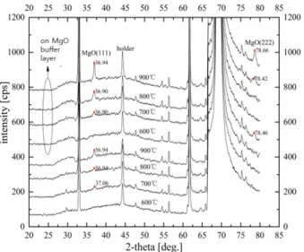
Fig. 2. (Color online) The XRD diffraction patterns of the MgO film on Si(100) substrates, which were annealed at different temperature.
set of experiments were performed using the Si(100) sub- strate without RF magnetron sputtering process.
The phase structure of the films was examined by X-Ray diffraction (XRD) using the Cu Kα radiation.
The surface morphology of the films was investigated with atomic force microscopy (AFM). Transmission elec- tron microscope (TEM) was used to investigate the mi- crostructure of the surface and cross section
III. RESULTS AND DISCUSSION
XRD results showed that (111)-oriented MgO films were obtained by combining RF magnetron sputtering and sol-gel process. This may due to the higher growth rate for the 111 faces [2]. Some other reports indicate the dependence of film orientations on the substrate temper- ature during deposition for the orientation of the MgO film on Si(100) substrate [1,8,9]. They show that the for- mation of a SiO2layer during heat-temperature is some- what inevitable for sol-gel derived crystalline films even though the Si substrates have been etched to remove the residual oxide. From this aspect, the (111) growth ori- entation of the MgO film may be also related to the formation of the SiO2 inter-layer.
As showed in Fig. 2, a tiny amorphous diffraction peak appeared on the bottom of the films when annealing tem- perature achieved 600 ◦C. It indicated that the crystal- lization of MgO films was not complete. As the anneal- ing temperature increased to 700 ◦C, 800 ◦C and 900
Fig. 3. (Color online) The relation between FWHM and the normalized MgO (111) intensity and annealing tem- perature according to the existence of buffer layer.
◦C, (111) preferred orientation became more and more obvious. Compared with the samples which had none buffer layer, the (111) orientation of MgO film which was based on MgO buffer layer occurred easily from 700
◦C. The diffraction peak became stronger with the in- crease of the annealing temperature. It can clearly show at Fig. 3 that the normalized intensity of (111) orienta- tion of MgO change with the annealing temperature and the existence of MgO buffer layer. The sample deposited on MgO buffer layer that annealed at 900◦C shows the highest normalized (111) intensity. It indicated that in- troducing MgO buffer layer improved the crystallization of MgO films significantly.
Also, Fig. 3 showed the relation between FWHM and annealing temperature. According to Fig. 3, at 700 ◦C, the corresponding FWHM obtained from MgO film of buffer layer became significantly smaller and it reveal the the crystallinity of MgO films was improved. However, as the annealing temperature increasing, the FWHM show similar values regardless of the existence of buffer layer.
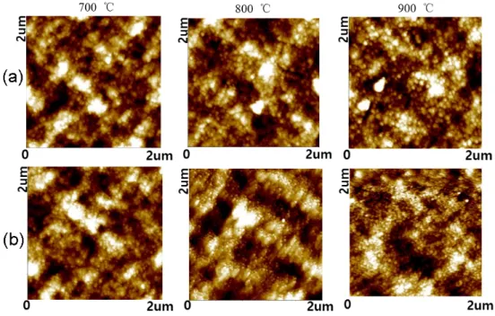
Investigations of the films surface morphology per- formed by AFM showed grain behavior as annealing tem- perature increased. According to Fig. 4, the film which had big clusters and blurred rough uneven surface could be obtained when the annealing temperature was not high. It was probably due to low temperatures, the atoms on the Si substrate cannot absorb enough energy to diffuse and the weak interaction during crystallization process resulted in an inconspicuous crystallization.
Fig. 4. (Color online) AFM results of the MgO films which were grown on (a) Si(100) substrates and (b) buffer layer.
Fig. 5. (Color online) The relation between RMS and grain size. Solid line and dashed line represented the data of film which had MgO buffer layer and none buffer layer, respectively.
Under certain extent, the increase of the annealing temperature accelerated the growth of the film. The par- ticles became uniform and the boundary became much clearer. MgO particles arranged orderly and the sur- face defects were reduced. The MgO film became much smooth. That indicated the quality of the film was get- ting better.
Fig. 5 showed the relation between FWHM and an- nealing temperature. With the annealing temperature increasing, the RMS roughness became smaller and the
grain size became larger in a certain limit. Once the temperature increased over the limit, the RMS rough- ness and the grain size inversely changed. As for the MgO film which was prepared only by sol-gel method, the best temperature for the larger grain size and rela- tive smaller RMS roughness was around 700◦C. By such analogy, the best temperature for the MgO film which was based on MgO buffer layer was about 800◦C.
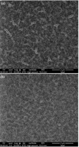
According to Fig. 6, the surface of the samples became much more smooth after introducing buffer layer. The cracking phenomenon had been effectively reduced.
TEM was used to investigate the surface and cross sec- tion of the samples. According to Fig. 7, a clear buffer layer could be observed. Crystalline state and dense mi- crostructure were obvious. The average thickness of the prepared MgO film was about 153 nm, which is coated 8 times and annealed at 900◦C. Moreover, Fig. 8 showed the high resolution TEM images about partial enlarged area of MgO buffer layer. In the MgO buffer layer, the MgO lattice fringes can be investigated and the distance of MgO (200) crystal face was about 2.10 Å.
IV. CONCLUSION
Highly (111)-oriented MgO thin film has been pre- pared on Si(100) substrate by combining RF sputtering
Fig. 6. The surface of the samples investigated by SEM.
and sol-gel process. From the annealing temperature at 700 ◦C, the crystallization of MgO occurred to some ex- tent. Regardless of the existence of the MgO buffer layer, the increase of the annealing temperature improves the growth of (111) orientation significantly. Based on MgO buffer layer, the MgO (111) peaks easily occurred from 700 ◦C and the crystallization of MgO films was rapidly improved by the increase of the annealing temperature.
However, at higher annealing temperatures than 700◦C, in spite of the existence of buffer layer, the structural properties of MgO films are almost same as those of MgO films formed on no buffer layer.
ACKNOWLEDGEMENTS
This research was supported by Basic Science Research Program through the National Research Foundation of Korea (NRF) funded by the Ministry of Education, Sci- ence and Technology (2012R1A1A4A01011424).
Fig. 7. (Color online) Bright field TEM image of the sample which was grown on MgO buffer layer.
Fig. 8. High resolution TEM images about partial en- larged area of MgO buffer layer.
REFERENCES
[1] J.-G. Yoon and K. Kim, Appl. Phys. Lett. 66, 2661 (1995).
[2] W. J. DeSisto and R. L. Henry, Appl. Phys. Lett.
56, 2522 (1990).
[3] J. G. Lisoni, M. Siegert, C. H Lei, W. Biegel and J.
Schubert et al., Thin Solid Films 389, 219 (2001).
[4] B. Mazumder, V. Purohit, M. Gruber, A. Vella and F. Vurpillot et al., Thin Solid Films 589, 38 (2015).
[5] D. Velázquez, R. Seibert, Z. Yusof, J. Terry and L.
Spentzouris, Bull. Am. Phys. Soc. 60, 1846 (2015).
[6] J. Wollschläger, J. Viernow, C. Tegenkamp, D.
Erdös and K. M Schröder Appl. Surf. Sci. 142, 129 (1999).
![Fig. 1 represents the basic procedure of the experi- experi-ment. The precursor solution of MgO, about 0.2 M con-centration, was prepared by dissolving magnesium ethox-ide in 2-methoxyethanol [8, 10]](https://thumb-ap.123doks.com/thumbv2/123dokinfo/5422496.228415/2.892.78.419.159.366/represents-procedure-precursor-solution-centration-dissolving-magnesium-methoxyethanol.webp)