Abstract
This work presents a low-power CMOS image sensor (CIS) with a multi-column-parallel (MCP) readout structure while focusing on improving its performance compared to previous works. A delta readout scheme that utilizes the image characteristics is optimized for the MCP readout structure. By simply alternating the MCP readout direction for each row selection, additional memory for the row- to-row delta readout is not required, resulting in a reduced area of occupation compared to the previous work. In addition, the bias cur- rent of a pre-amplifier in a successive approximate register (SAR) analog-to-digital converter (ADC) changes according to the operating period to improve the power efficiency. The prototype CIS chip was fabricated using a 0.18-µm CMOS process. A 160 × 120 pixel array with 4.4 µm pitch was implemented with a 10-bit SAR ADC. The prototype CIS demonstrated a frame rate of 120 fps with a total power consumption of 1.92 mW.
Keywords: CMOS image sensor (CIS), Successive approximate register (SAR), Analog-to-digital converter (ADC), Image property, Delta readout scheme.
1. INTRODUCTION
Currently, customer demands for CMOS image sensor (CIS)- based applications are growing rapidly [1,2]. In particular, multiple CISs are mounted as electronic eyes on personalized portable devices such as mobile phones and healthcare applications. Because such electronic devices are mostly powered by batteries, maintaining low power consumption has become an important design issue for imaging sensor systems.
For analog-to-digital (A/D) conversion of signals, there are various types of readout analog-to-digital converters (ADCs):
single-slope (SS) ADC, sigma-delta (∑-Δ) ADC, successive approximate register (SAR) ADC, and cyclic (CY) ADC [3]-[6].
Among them, the SAR ADC has been in the spotlight for low- power readout because it does not consume static power.
However, its capacitive digital-to-analog converter (C-DAC) for generating a full A/D reference requires a large area, making it difficult to design a layout in a narrow column pitch. Moreover,
because the pixel pitch becomes smaller for high pixel resolution, the same problem is encountered in other types of column-parallel (CP) readout ADCs. Here, the pixel pitch is equal to the column pitch in the CP readout structure. To overcome this disadvantage, multi-column-parallel (MCP) readout structures in which one readout ADC covers several columns have been reported [7-9].
Recently, in addition to the studies on traditional circuit techniques for low-power design, various studies [8-11] utilizing the characteristics of the input signal have been reported to obtain further performance improvement. In a previous work [8], based on the image properties, a delta readout scheme that reads only the signal difference between two adjacent pixels (Δ px ) has been proposed for a power-efficient readout with SAR ADCs. After completing the A/D conversion for the previous pixel by utilizing its most significant bits (MSBs) MSB information, the C-DAC of the SAR ADC is not fully reset; only the remaining least signal bits (LSBs) are reset. MSBs are memorized and then re-switched in C-DAC for the next A/D conversion. Because the MSB information from the previous pixel is highly correlated with a selected pixel, the number of conversion steps is effectively reduced, resulting in a low-power readout.
In this work, with the same motivations as previous studies, we propose a more optimized delta readout algorithm for rolling- shutter readout CISs adopting the MCP readout structure.
Compared to prior studies [8,9], this work considers the row-to- row correlation when changing the row to readout the pixel information (as in rolling shutter readout mechanism). Furthermore,
1
School of Electrical Information Communication Engineering, Kangwon National Unversity, 346 Jungang-ro, Samcheok-si, Gangwon-do 25913, Republic of Korea
+
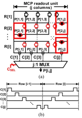
![Fig. 1 shows a simplified schematic of the MCP readout structure [8,12], which uses one readout ADC per multiple columns](https://thumb-ap.123doks.com/thumbv2/123dokinfo/4790176.276968/2.892.481.799.141.602/shows-simplified-schematic-readout-structure-readout-multiple-columns.webp)