Nanocrystalline Si formation inside SiN
xnanostructures usingionized N
2gas bombardment
Min-Cherl Jung1, Young Ju Park2, Hyun-Joon Shin1, Jun Seok Byun3, Jae Jin Yoon3, and Yongsup Park*3
1Beamline Department, Pohang Accelerator Laboratory, POSTECH, Pohang 790-784
2Nano-device Research Center, Korea Institute of Science and Technology, Seoul 136-79
3Department of Physics, Kyung Hee University, Seoul 130-701
(Received October 11 2007)
Nanostructures of SiNx were made by bombardment of ionized N2 on Si surfaceand subsequent annealing. Atomic force micrograph showed the density of SiNx nanostructures was 3×10¹⁰/cm2. Their lateral size and height were 40~60 nm and 15 nm, respectively. The chemical state of the nanostructure was measured using X-ray photoelectron spectroscopy, which changed from SiNx to Si3N4 + SiNx as the bombarding ionized gas current increases.
Upon annealing, transmission electron micrograph showed a clear evidence for crystalline Si phase formation inside the SiNx nanostructures. Photoluminescence peak observed at around 400 nm was thought to be originated from the interface states between the nanocrystalline Si and surrounding SiNx nanostructures
KEYWORDS:Si nanostructures, ion beam bombardment, XPS, SiNx, photoluminescence
Ⅰ. Introduction
Recently, Si-based luminescent nanostructures such as nanocrystalline Si (nc-Si) have been investigated intensively for optoelectronic device applications [1-4]. In particular, many researchers have reported fabrication methods based on plasma-enhanced chemical vapor deposition (PECVD) and ion implantation [3] for the formation and control of Si-based nanostructures. A typical formation mechanism for the nc-Si is based on a self-organization process:
transformation of non-stoichiometric SiNx or SiOx thin layers on a silicon substrate into ns-Si embedded in stoichiometric Si3N4 or SiO2 through the post-growth thermal annealing processes [1,5]. We have previously reported that SiNx nanostructures with average lateral size of 40 nm and the height of 5 nm could be formed
on a clean silicon surface by bombarding ionized N2
gas and post-annealing [5]. Starting from SiO2
covered Si substrate and using a similar method, we have also shown that SiO2 nanostructures and bare Si surface were formed underneath SiNx capping layer.
Thermal annealing produced nc-Si in the SiNx layer only on bare Si region [6].
In this paper, we report the formation of nc-Si inside SiNx. The initial SiNx nanostructure was formed by controlled bombardment of ionized N2 gas.
The nc-Si was then created by post-annealing the nanostructure as evidenced by transmission electron micrograph. The 400 nm photoluminescence peak observed was attributed to the interface states between the nanocrystalline Si and the SiNx capping layer.
Nanocrystalline Si formation inside SiNx nanostructures usingionized N2gas bombardment
Intensity (arb. unit)
106 104 102 100 98 Binding Energy (eV)
404 400 396 392
Binding Energy (eV)
Clean 0 .0 4 0 .1 0 .3 0 .5 1 .0 2 .0 2 .0 ( a n n e a l i n g - 1 m i n | 1 0 0 0 ° C )
C l e a n 0 .0 4 0 .1 0 .3 0 .5 1 .0 2 .0 2 .0 ( a n n e a l i n g - 1 m i n | 1 0 0 0 ° C )
N 1 s
Si 2p
(a) ( b )
Ⅱ. Experimental Methods
We used commercially available (001) orientated silicon wafer for substrates, which were Sb-doped with a resistivity of 0.01 -cm. The native oxide layer on Si was removed using RCA process in air before the wafers were put into the ultra-high vacuum (UHV) chamber (background pressure 1 ×10⁻¹⁰ Torr).
The vacuum system was composed of an analysis chamber for the X-ray photoelectron spectroscopy (XPS) experiment, and an ion beam treatment chamber for the surface modifications. Samples were exposed to the ionized N2 gas (N2 99.999 %) using a hot-filament ion gun at room temperature. To obtain various sample current densities, the gas pressure was changed from 1.0× 10⁻⁸ to 1.0×10⁻⁶ Torr as well as the beam energy from 0.5 to 3 keV. The bombardment time was maintained at 30 min for all samples. Physico-chemically modified silicon surfaces were investigated by XPS and atomic force microscopy (AFM). The Si 2p, O 1s and N 1s core-level spectra and the binding energy 99.3 eV of Si 2p3/2 for the clean silicon were obtained by referencing Au 4f7/2 peak. The structural analysis was performed using high-resolution transmission electron microscopy (HR-TEM), and the luminescent properties of the nc-Si were determined using photoluminescence (PL) measurement.
Ⅲ. Results and Discussions
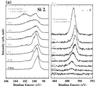
Figures 1(a) and 1(b) show Si 2p and N 1s XPS core-level spectra respectively with various ion current densities. As the sample current density increased, a broad peak clearly appeared at the binding energy range 100.0~102.0 eV in Si 2p core-level spectrum. The intensity of N 1s core-level similarly increased with increasing sample current density. Although not shown, there was no sign of O
FIG. 1. (a) Si 2p and (b) N 1score-level spectra with various N2+ions current density ranging from 0.04 to 2.0 mA/cm2. The top spectrum is for the sample formed by the current density of 2.0 mA/cm2 but annealed in N2 gas environment of 1.0×10⁻⁸ Torr at 1000 ℃ for 1 min.
1s core-level peak, implying that oxygen impurity was not incorporated. The broad shape of the Si 2p peakwas ascribed to the formation of SiNx with various x values [1,5]. After annealing this sample at 1000 ℃ for 1 min in N2 gas of 1.0 × 10⁻⁸ Torr, the spectral intensity of Si 2p peak at~102.0 eV significantly increased as seen in the top spectrum in Fig. 1(a). This means that chemical states on the surface were transformed to a more stable state such as Si3N4 with the binding energy of 101.8 eV [1]. The peak intensity and width of N 1s core-level spectrum also increased after the annealing. It should be noted that the positions of N 1s peak for the samples with current density 0.04~0.3 ㎂/㎠ were at the higher binding energy than those of other samples. This is the evidence that the chemical state of the samples with these ion current density ranges is that of SiNx
by adsorption of nitrogen atom on Si [1].For the samples with higher ion current density, we confirmed from Si 2p and N 1s core-level spectra that the chemical states are those of SiNx + Si3N4.
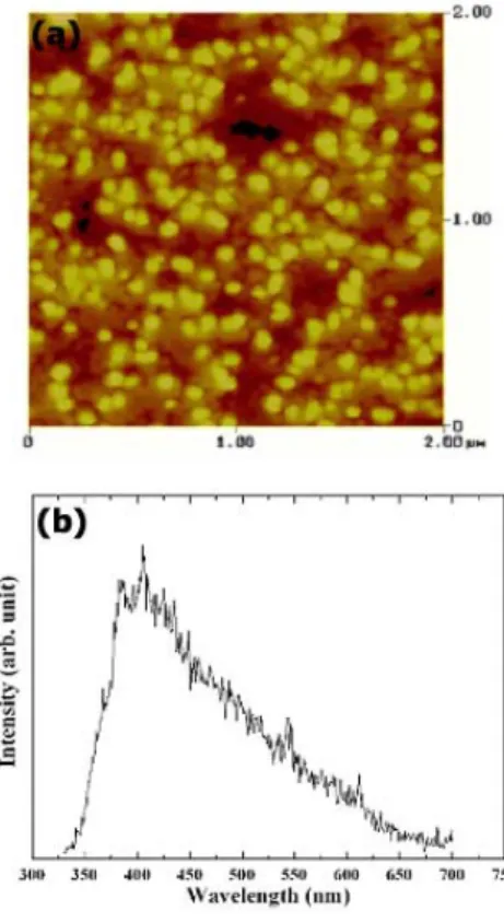
FIG. 2. (a) The AFM image for the annealed sample in Fig. 1. The lateral size and the height of nanostructures is 40~60 nm and 15 nm, respectively. (b) Room temperature PL spectrum for the annealed sample. Emission peak at around 400 nm is clearly visible.
Figures 2(a) and (b) show the AFM surface morphology and the room temperature photoluminescence (RT-PL) spectrum respectively for the sample formed using 2.0 mA/cm2 of N2 ion current density, and subsequently annealed at 1000 ℃ for 1 min in 1.0 × 10⁻⁸ Torr of N2
gas environment. In the AFM image, randomly distributed nanostructures were observed on the surface.
The lateral size and the height of nanostructures are 40~60 nm and 15 nm on average, respectively. The areal density of the nanostructures is 3×10¹⁰ /cm2. It is noted that nanostructures formed by the ionized gas with the some kinetic energy are composed of SiNx components and their shape is governed by the interactions at the interfaces. The differences in surface and interface energies between dissimilarmaterials such as Si3N4, SiNx, and nc-Si are thought to be origin of the
formation of observed nc-Si.
As shown in Fig. 2(b), RT-PL peak at the wavelength around 400 nm was obtained from the annealed sample. In order to confirm the origin of the luminescence, anHRTEM image of the cross-sectional view of the annealed sample was taken, as shown in Fig. 3. We found the nc-Si in SiNx + Si3N4
nanostructure. In the cross-sectional view, it is clearly seen that the nc-Si was located inside the nanostructures with the lateral size of 30 nm and the height of 10 nm. Although there is a possibility that the cross-sectional view offered an overlap of many nc-Si image with much smaller sizes, we could not draw definite conclusion. Therefore, we believe it is more reasonable to conclude that the observed PL spectra is due to the interface states that are formed between the nc-Si and SiNx nanostructures or some defects in the Si structures and not due to the nc-Si clusters of sizes 3~4 nm. Finally, the mechanism of the creation of nc-Si in this work is firstly SiNx nanostructures with the chemically metastable states are formed by the ionized N2 gas at room temperature; secondly nc-Si’s are created in SiNx
nanostructures after annealing in ultra-high vacuum. During the annealing process, the chemically metastable states of SiNx are transformed to the chemically stable Si3N4. The rest of Si atoms are transformed to nc-Si in the structural confinement around the chemical barrier of Si3N4.
FIG. 3. The cross-sectional HRTEM images for the annealed sample. The crystalline phase of the Si is easily visible inside the nanostructures.
Nanocrystalline Si formation inside SiNx nanostructures usingionized N2gas bombardment
Ⅳ. Conclusions
The nc-Si’s inside Si nitride nanostructures were formed by the ionized N2 gas. The Si-nitride nanostructures have the chemical states of SiNx and Si3N4 mixture above the ion current density of 0.5 mA/cm2. The nc-Si’s with the lateral size of 30 nm and the height of 10 nm were located inside the nanostructures. We believe it is more reasonable to conclude that the observed PL spectra peaked at 400 nm is due to the interface states that are formed between the SiNx nanostructures and the nc-Si clusters of sizes much larger than 3~4 nm. The process described here offers an easy method for high density of nc-Si formation using ionized gas that is easily produced using commonly available ion guns.
Acknowledgement
MCJ and YP were partially supported through grant
#F0004053 by the Information Display R&D Center, one of the 21st Century Frontier R&D Programs funded by MCIE of the Korean Government.
References
[1] J. Robertson, Nature 418, 30 (2002).
[2] S. Srirman, S. Agarwal, E. S. Aydil and D.
Maroudas, Nature 418, 62 (2002).
[3] G. F. Grom, D. J. Lockwood, J. P. McCaffrey, H.
J. Labbé, P. M. Fauchet, B. White, Jr. J. Diener, D.
Kovalev, F. Koch and L. Tsybeskov, Nature 407, 358 (2000).
[4] L. Pavesi, L. Dal Negro, C. Mazzoleni, G. Franzó and F. Priolo, Nature 408, 440 (2000).
[5] M.-C. Jung and M. Han, Jpn. J. Appl. Phys. 43, 1127 (2004).
[6] M.-C. Jung, T. G. Lee, Y. J. Park, S. H. Jun, J. Lee, M. Han, J. S. Jeong and J. Y. Lee, Appl. Phys. Lett.
82, 33653 (2004).
이온화 N
2가스 입사를 이용한 SiN
x나노구조 내부의 Si 나노결정 형성
정민철1ㆍ박용주2ㆍ신현준1ㆍ변준석3ㆍ윤재진3ㆍ박용섭*3
1포항방사광가속기 연구소 빔라인부, 포항 790-784
2한국과학기술 연구원 나노소자 연구 센터, 서울 136-791
3경희대학교 이과대학 물리학과, 서울 130-701
(2007년 10월 11일 받음)
실리콘 표면에 이온화된 N2가스를 입사한 후 어닐링을 통해서 SiNx나노구조를 형성하였다. 원자힘 현미경으로 관찰한 결과 이 나노구조의 밀도는 3×10¹⁰/cm2 였으며, 가로 크기는 40~60 nm 이고 높이는 약 15 nm 임을 알 수 있었다. 엑스선 광전자 분광기술을 이용하여 이 나노구조의 화학상태를 측정하였는데, 입사하는 이온화된 N2의 단위시간당 양이 증가함에 따라서 화 학상태가 SiNx에서 Si3N4 + SiNx 형태로 변화함을 알 수 있었다. 열처리를 한 시료를 투과전자 현미경으로 측정된 결과는 SiNx 나노구조를 내부에 Si 나노 결정이 형성된 것을 보여주었다. 광여기 발광특성에서 관찰된 400 nm파장의 스펙트럼은 Si 나노결정의 크기를 고려할 때 나노결정과 SiNx 나노구조 사이의 계면상태에서 기인한 것으로 생각된다.
주제어:Si 나노구조, 이온빔 입사, XPS, SiNx, PL E-mail address:[email protected]