Increase in indium diffusion by tetrafluoromethane plasma treatment and its effects on
the device performance of polymer light-emitting diodes
Sung Jin Jo, Chang Su Kim, Jong Bok Kim, Seung Yoon Ryu, Joo Hyon Noh, Hong Koo Baik, , Youn Sang Kim, and Se-Jong Lee
Citation: Journal of Applied Physics 103, 114502 (2008); doi: 10.1063/1.2939261 View online: http://dx.doi.org/10.1063/1.2939261
View Table of Contents: http://aip.scitation.org/toc/jap/103/11 Published by the American Institute of Physics
Increase in indium diffusion by tetrafluoromethane plasma treatment and
its effects on the device performance of polymer light-emitting diodes
Sung Jin Jo,1Chang Su Kim,1Jong Bok Kim,1Seung Yoon Ryu,1Joo Hyon Noh,1 Hong Koo Baik,1,a兲 Youn Sang Kim,2and Se-Jong Lee3
1
Department of Materials Science and Engineering, Yonsei University, Seoul 120-749, Republic of Korea 2Center for Intelligent Nano-Bio Materials, Division of Nano Sciences and Department of Chemistry, Ewha Womans University, Seoul 120-750, Republic of Korea
3Department of Materials Science and Engineering, Kyungsung University, Busan 608-736, Republic of Korea
共Received 15 January 2008; accepted 9 April 2008; published online 5 June 2008兲
The effects of tetrafluoromethane 共CF4兲 plasma treatment of indium-tin-oxide 共ITO兲 anode on
indium diffusion into a poly共3,4-ethylene dioxythiophene兲:poly共styrene sulphonate兲 共PEDOT:PSS兲 layer were studied. Auger electron spectroscopy共AES兲 depth profile showed that 0.2 at. % indium was present in the PEDOT:PSS layer when ITO was not plasma treated. The plasma treatment of ITO increased the indium concentration to⬃6 at. %. The increase in indium can be explained by an oxygen deficiency in the CF4plasma treated ITO. The presence of indium in the PEDOT:PSS layer
showed a correlation with performance degradation of polymer light-emitting diodes. © 2008 American Institute of Physics.关DOI:10.1063/1.2939261兴
I. INTRODUCTION
Polymer light-emitting diodes 共PLEDs兲 are considered promising candidates for full color, cheap, and flexible dis-plays, which are easy to process.1,2A PLED consists of an emitting polymer layer that is sandwiched between an anode and a cathode. A great deal of effort has been made towards improving the performance of the PLEDs.
One approach is to modify the surface properties of in-dium tin oxide 共ITO兲 with various techniques, such as plasma treatment,3,4 ultraviolet-ozone cleaning,5 mechanical polishing,6 and coating treatment with a self-assembled monolayer.7Plasma treatment is regarded as the most prom-ising technique, since it results in high work function as well as smooth surface. Another approach is to insert carrier injecting/transport material in between the electrode and emissive polymer layer, so that the carriers can be effectively transported to the emission zone.8–10Poly共3,4-ethylene diox-ythiophene兲:poly共styrene sulphonate兲 共PEDOT:PSS兲 is one of the best known hole injecting material, mainly because of its excellent electrical conductivity and eletro-optic proper-ties as well as processability. However, it has been shown that the interface between ITO and PEDOT:PSS is not stable, with indium contaminating the polymer.11,12 Due to the strong acidic nature of PSS, a typical aqueous PEDOT:PSS solution has an acidity of pH = 1.2, and In2O3has a relatively
high solubility in acid.13 For PEDOT:PSS on ITO, it is re-ported that the acidic PEDOT:PSS solution can etch ITO during the polymer spin coating process. It is, therefore, im-portant to investigate the ITO/PEDOT:PSS interface property in order to achieve a higher performance in PLEDs, espe-cially when the ITO is plasma treated. However, among ex-isting studies on ITO/PEDOT:PSS interfaces, only a few have considered the effects of plasma treatment on indium
diffusion. This report is on the effects and influence of plasma treatment on indium diffusion and the electrical prop-erties of PLEDs.
II. EXPERIMENTAL
ITO coated glass was used as the substrate and it was approximately 200 nm thick with a sheet resistance of ap-proximately 15⍀/square. The ITO was first cleaned in trichloroethylene, acetone, and isopropyl alcohol in an ultra-sonic bath, rinsed in de-ionized water, and finally dried in a high purity N2 gas stream. The ITO substrate was then
tet-rafluoromethane 共CF4兲 plasma treated in a
capacitance-coupled-plasma etcher for 5 min at rf power of 100 W. The electrodes were made of Cu and had dimensions of 5 ⫻10 cm2. The upper electrode was grounded and the rf
power was connected to the bottom electrode. The pressure of the chamber and the flow rate of the CF4were 150 mTorr
and 15 SCCM 共SCCM denotes cubic centimeter per minute at STP兲, respectively.
PEDOT:PSS was spin coated approximately 50 nm thick as a hole transport layer. The residual solvent was removed by drying at 200 ° C on a hot plate or suction under vacuum at room temperature. Directly afterwards, poly共9,9-dioctyl-fluorene兲 共PFO兲 was spin coated from its toluene solution at a concentration of 1 mg ml−1onto the PEDOT:PSS films as a light-emitting layer. A bilayer cathode consisting of a LiF layer and an Al layer was deposited at 10−6Torr by thermal evaporation. The device structure consists of ITO
共200 nm兲/PEDOT:PSS 共50 nm兲/PFO 共80 nm兲/LiF
共3 nm兲/Al 共100 nm兲. The emitting area was defined to be 9 mm2. The current-voltage 共I-V兲 measurements were all carried out in air using a Keithley 2400 source meter, and the luminescence-voltage 共L-V兲 characteristics were measured with a calibrated silicon photodiode using a Keithley 487. The dependence of the indium diffusion on the heat treat-a兲Electronic mail: [email protected].
ment time was determined by the Auger electron spectros-copy 共AES兲 depth profile. AES measurements were per-formed on a PHI 610 scanning Auger microprobe. The base pressure in the analysis chamber was 3⫻10−10torr. A
pri-mary electron beam with energy of 10 keV and a current of 0.02⍀A was incident on the sample surface.
III. RESULTS AND DISCUSSION
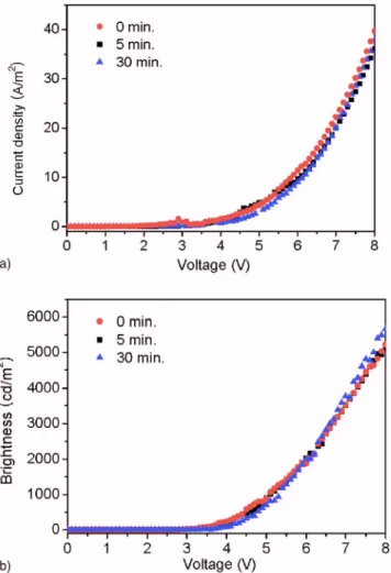
Figure1 shows the I-V-L characteristics of PLEDs with various baking times of PEDOT:PSS when ITO was CF4 plasma treated. The I-V performance of the device was found to be strongly dependent on the baking time of PEDOT:PSS. The device with vacuum dried PEDOT:PSS exhibited the maximum current density. With further increment in baking time, the current density was gradually decreased. The cor-responding L-V measurement presented a similar behavior because luminance intensity was determined by current den-sity. The device with vacuum dried PEDOT:PSS revealed the maximum brightness at the same driving voltage. Figure 2 shows the characteristics of I-V-L for PLEDs with various baking times of PEDOT:PSS when ITO was not CF4plasma
treated. No obvious change in the performance was observed after the baking, which indicated that the PEDOT:PSS layer was not damaged in the baking process. In addition, these experimental results showed that the ITO anodes treated with
CF4 plasma resulted in significant differences in the electri-cal characteristics, which became even worse as the baking time increased.
In typical PLED with ITO/PEDOT:PSS/PFO/LiF/Al structure, the barriers for the electron and hole injections are important because the barriers determine the I-V characteris-tic of the device.14 In our previous work, the work function of CF4 plasma treated ITO was increased from 4.81 to 5.35 eV. The increase in work function was due to the removal of carbon contaminants as well as adsorption of fluorine on the ITO surface by CF4plasma treatment.15This
led to a decrease in the barrier height of the anode between ITO and PEDOT:PSS. As a result, the current and lumines-cence for the device fabricated on CF4 plasma treated ITO
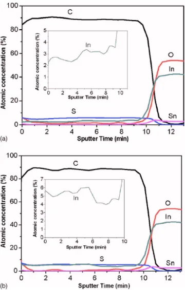
were much higher than those of the untreated ITO. However, the performance of the device fabricated with CF4 plasma treated ITO was worse than that of the untreated ITO as the baking time of PEDOT:PSS increased. The hole injection barrier is believed to be affected by the baking time of the PEDOT:PSS layer. AES measurements were performed to investigate the effects of the baking time. Figures 3 and 4 show the AES depth profile of ITO/PEDOT:PSS, and the inset indicates the indium concentration in the PEDOT:PSS layer. A depth profile was taken from the PEDOT:PSS to-ward the ITO. The change in the most abundant element
FIG. 1.共Color online兲 Effects of baking time of PEDOT:PSS on the perfor-mance of PLEDs when ITO was CF4plasma treated:共a兲 current density vs
applied voltage and共b兲 EL intensity vs applied voltage.
FIG. 2.共Color online兲 Effects of baking time of PEDOT:PSS on the perfor-mance of PLEDs when ITO was not CF4plasma treated:共a兲 current density
vs applied voltage and共b兲 EL intensity vs applied voltage.
from C to O determined the location of the PEDOT:PSS/ITO interface region. AES measurements showed that about 0.2 at. % indium was present in the PEDOT:PSS layer and that the concentration increased slightly as the baking time increased. A comparison between Figs. 3 and4 shows that there was a considerable increase in the amount of indium in the PEDOT:PSS layer when ITO was CF4 plasma treated. The CF4 plasma treated sample gave an indium content of
about 3 at. % and the indium content was raised to about 6 at. % by prolonged heat treatment. Prolonged heating in-duced a further intake of indium in the PEDOT:PSS layer, either due to a continued etching reaction or the diffusion of previously formed etch products from the ITO/PEDOT:PSS interface.16,17Indium diffusion may be related to the surface state of ITO. It is likely that indium diffusion under heat treatment is associated with indium migration of indium at-oms from oxygen-deficient ITO. In our previous work, oxy-gen deficiency was observed in CF4 plasma treated ITO.18
Indeed, we found that CF4plasma treatment of ITO led to an
increase in indium incorporation by a factor of 10.
The presence of indium in the PEDOT:PSS may change the electrical properties, especially the charge injection, of the PLED.19 In order to understand the influence of the in-dium diffusion on device performance, hole-only devices
共ITO/PEDOT:PSS/PFO/Au兲 were made. Hole-only devices are particularly useful to study hole injection from various PEDOT:PSS layers. The barrier for hole injection is given by the difference between the PEDOT:PSS Fermi energy and the light-emitting polymer highest occupied molecular or-bital level. I-V characteristics for the hole-only device are shown in Fig. 5. As the baking time increases, the IP of PEDOT:PSS decreases and the hole injection barrier creases. The hole-only current decreases markedly as the in-dium content in PEDOT:PSS increases. Since all the compo-nents of the hole-only device except PEDOT:PSS are the same, the lower current should be correlated with an in-creased barrier of the PEDOT:PSS. Thus, the hole-only vice can prove the influence of indium diffusion on the de-vice performance. This is in good agreement with the results shown in Fig. 1for plasma treated PLEDs.
A possible cause for device degradation is considered to be the dedoping of PEDOT in PEDOT:PSS due to reaction of ITO with protons in PSS and those in doped PEDOT. Re-cently, Chang and Chen showed that protons in PEDOT:PSS can react with ITO in the presence of water to yield indium salt, leading to a change in its ionization potential, and that the indium ions can diffuse into the PEDOT:PSS layer.20
FIG. 3.共Color online兲 AES depth profile of ITO/PEDOT:PSS sample when ITO was not CF4plasma treated:共a兲 without baking and 共b兲 30 min baking.
FIG. 4.共Color online兲 AES depth profile of ITO/PEDOT:PSS sample when ITO was CF4plasma treated:共a兲 without baking and 共b兲 30 min baking.
Thus, the indium content in PEDOT:PSS is related to the charge injection property and is a possible cause for device degradation.
IV. CONCLUSION
AES depth profile shows that the indium diffused almost throughout the entire PEDOT:PSS layer and that prolonged heating further induced the intake of indium in the PEDOT-:PSS layer. We also found that the oxygen deficiency in CF4
plasma treated ITO led to an increase in indium incorpora-tion. It is shown that the charge injection property is affected by indium content in the PEDOT:PSS. The presence of in-dium in the PEDOT:PSS layer showed a correlation with performance degradation of PLEDs. Therefore, drying of the spin cast PEDOT:PSS by vacuum suction is a more desirable process when ITO is CF4 plasma treated. Also, remote
plasma treatment and plasma polymerization of fluorocarbon are possible methods to improve work function properties without degrading the device.
1J. H. Burroughes, D. D. C. Bradley, A. R. Brown, R. N. Marks, K.
Mackey, R. H. Friend, P. L. Burn, and A. B. Holmes,Nature共London兲 347, 539共1990兲.
2D. Braun and A. J. Heeger,Appl. Phys. Lett.58, 1982共1991兲.
3C. C. Wu, C. I. Wu, J. C. Sturm, and A. Kahn,Appl. Phys. Lett.70, 1348
共1997兲.
4I. Chan and C. Hong,Thin Solid Films444, 254共2003兲.
5S. K. So, W. K. Choi, C. H. Cheng, L. M. Leung, and C. F. Kwong,Appl.
Phys. A: Mater. Sci. Process.68, 447共1999兲.
6F. Nuesch, L. J. Rothberg, E. W. Forsythe, Q. T. Le, and Y. Gao,Appl.
Phys. Lett.74, 880共1999兲.
7R. A. Hatton, S. R. Day, M. A. Chesters, and M. R. Willis,Thin Solid
Films394, 291共2001兲.
8S. A. van Slyke, C. H. Chen, and C. W. Tang,Appl. Phys. Lett.69, 2160
共1996兲.
9J. Shi and C. W. Tang,Appl. Phys. Lett.70, 1665共1997兲.
10S. A. Carter, J. C. Scott, and P. J. Brock, Appl. Phys. Lett.71, 1145
共1997兲.
11A. R. Schlatmann, D. Wilms Floet, A. Hilberer, F. Garten, P. J. M.
Smul-ders, T. M. Klapwijk, and G. Hadziioannou,Appl. Phys. Lett.69, 1764 共1996兲.
12L. Ke, R. S. Kumar, K. Zhang, S. J. Chua, and A. T. S. Wee, Synth. Met.
140, 295共2004兲.
13D. R. Lide, CRC Handbook of Chemistry and Physics, 80th ed.共CRC,
Boca Raton, FL, 2000兲.
14I. D. Parker,J. Appl. Phys.75, 1656共1994兲.
15S. J. Jo, S. M. Jeong, W. J. Kim, W. H. Koo, S. H. Choi, C. S. Kim, S. J.
Lee, and H. K. Baik,J. Vac. Sci. Technol. A23, 1367共2005兲.
16M. P. de Jong, L. J. van IJzendoorn, and M. J. A. de Voigt,Appl. Phys.
Lett.77, 2255共2000兲.
17K. W. Wong, H. L. Yip, Y. Luo, K. Y. Wong, W. M. Lau, K. H. Low, H.
F. Chow, Z. Q. Gao, W. L. Yeung, and C. C. Chang,Appl. Phys. Lett.80, 2788共2002兲.
18S. J. Jo, C. S. Kim, S. Y. Ryu, J. B. Kim, J. H. Noh, S. J. Lee, and H. K.
Baik, Jpn. J. Appl. Phys., Part 1 46, 6814共2007兲.
19S. T. Lee, Z. Q. Gao, and L. S. Hung,Appl. Phys. Lett.75, 1404共1999兲. 20C. Chang and S. Chen,Appl. Phys. Lett.91, 103514共2007兲.
FIG. 5.共Color online兲 Current-voltage characteristics for hole-only devices 共ITO/PEDOT:PSS/PFO/Au兲.