ICCAS2005 June 2-5, KINTEX, Gyeonggi-Do, Korea
1. INTRODUCTION
Eddy current technique plays an important role in non destructive test. Based on the principal of electromagnetism, eddy currents flow in a conducting surface when time varying magnetic fields move through that surface. Magnetic fields induced from the surface could be detected by a coil placed in close proximity. As an example, assume that there is a deep crack in the surface immediately underneath the coil. This will interrupt or reduce the eddy current flow, thus decreasing voltage across the coil. We can then detect change in the material of interest. In the proper circumstances, eddy currents can be used for crack detection, material thickness measurements, coating thickness measurements and conductivity measurements, heat damage detection, case depth determination and heat treatment monitoring[1-2].
In this paper, eddy current techniques are used to nondestructively measure the thickness of nonconductive coatings on nonferrous metal substrates. A coil of fine wire conducting a high-frequency alternating current (above 0.1-10 MHz) is employed to set up alternating magnetic fields. When the probe is brought near a conductive surface, the alternating magnetic fields will set up eddy currents on the surface. The substrate characteristics and the distance of the probe from the substrate (the coating thickness) however affect the magnitude of the eddy currents. The eddy currents simultaneously create their own opposing electromagnetic field that can be sensed by the exciting coil itself or by a second, adjacent coil (detecting coil). The eddy current affects a voltage output of detecting coil. Any change in voltage of detecting coil can determine the distance between the probe and the substrate (the coating thickness).
2. METHOD
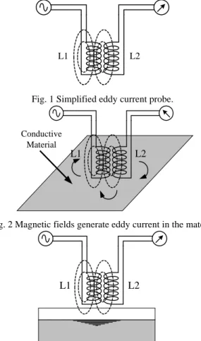
The basic of our eddy current testing is to monitor the voltages across the coil[3-5]. The proposed eddy current probe consists of a coil L1 and a coil L2 (see fig. 1). When alternating current is passed through the coil L1, a magnetic field is generated around the coil. The magnetic fields from coil L1 induce the voltage on the coil L2 which can be monitored on an AC meter. When ever the probe is brought in close proximity to a conductive material, such as aluminum,
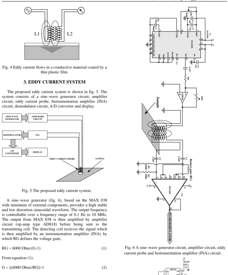
the alternating magnetic field generates a current in the material (see fig. 2) flowing in closed loops in a perpendicular plane with the magnetic flux. Such an eddy current decrease the magnetic induce to the coil L2 and also the voltage across coil L2 (see fig. 3 and 4). The distance that probe places from the conductive material is called lift-off which significantly affects the voltage across coil L2. The effect of lift-off can be used to measure the thickness of a nonconductive material coating on conductive material.
L2 L1
Fig. 1 Simplified eddy current probe.
L2 L1
Conductive Material
Fig. 2 Magnetic fields generate eddy current in the material.
L2 L1
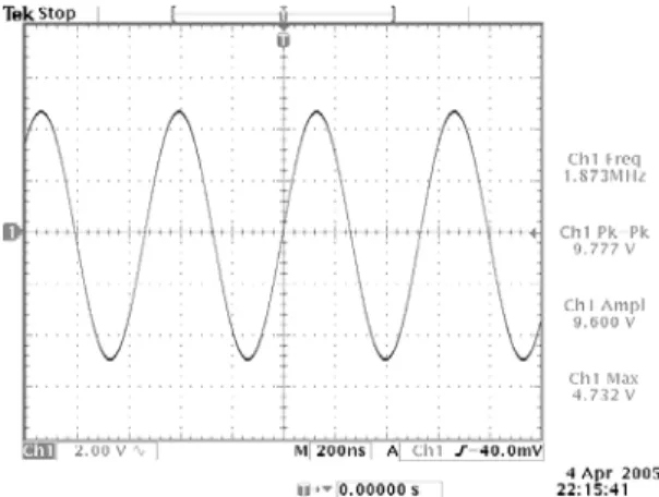
Fig. 3 Eddy current flows in a conductive material coated by a thick plastic film.
Eddy Current System For Coating Thickness Measurement
Apinai Rerkratn*, Jirayut Pulkham**, Kitiphol Chitsakul**, Manas Sangworasil**, Anucha Keawpoonsuk***
and Kiettiwan Songsataya***
*Electronics Research Center, Faculty of Engineering **Department of Electronics, Faculty of Engineering ***Department of Control Engineering, Faculty of Engineering
King Mongkut’s Institute of Technology Ladkrabang, Chalongkrung Rd, Ladkrabang, Bangkok, 10520, Thailand.
Tel +66 (0) 2739-0643, Fax +66 (0) 2739-2384, Email : [email protected]
Abstract: Coating thickness is an important variable that plays a role in product quality, process control, and cost control.
Measurement of film thickness can be done with many different instruments. In this paper, we introduce the new eddy current system for measure the thickness of nonconductive coatings on nonferrous metal substrates. The experimental results are shown that the proposed system is able to measure thickness of plastic film coating on aluminum plates in the range of 0 to 1000 microns with satisfy sensitivities, linearity, resolution and stability of the system.
Keywords: Eddy Current, Coating Thickness Measurement, Non Destructive Testing, Inductor
ICCAS2005 June 2-5, KINTEX, Gyeonggi-Do, Korea
L2
L1
Fig. 4 Eddy current flows in a conductive material coated by a thin plastic film.
3. EDDY CURRENT SYSTEM
The proposed eddy current system is shown in fig. 5. The system consists of a sine–wave generator circuit, amplifier circuit, eddy current probe, Instrumentation amplifier (INA) circuit, demodulator circuit, A/D converter and display.
DEMODULATOR SINE WAVE GENERATOR AMPLIFIER CIRCUIT INA A/D CONVERTER SAMPLE EDDY CURRENT PROBE
DISPLAY
Fig. 5 The proposed eddy current system.
A sine–wave generator (fig. 6), based on the MAX 038 with minimum of external components, provides a high stable and low distortion sinusoidal waveform. The output frequency is controllable over a frequency range of 0.1 Hz to 10 MHz. The output from MAX 038 is then amplified by amplifier circuit (op-amp type AD818) before being sent to the transmitting coil. The detecting coil recieves the signal which is then amplified by an instrumentation amplifier (INA) by which RG defines the voltage gain;
RG = 6000 Ohm/(G-1) (1) From equation (1);
G = [(6000 Ohm)/RG]+1 (2) Where G = Gain of instrumentation amplifier circuit. RG = Resistor used for define the gain of the
instrumentation amplifier.
Based on square law detection, the resultant DC signal has been demodulated from INA before being sent to A/D converter for converting to digital and displayed.
GND G NDG ND GND G ND PD 0 PD 1 SY N C DGND DV + OUT A0 V-V+ A1 RE F FADJ IN D ADJ CO S C MA X0 38 U1 MA X0 38 R1 12K C3 2 00p F N. C. N. C. C2 1nF C1 1uF VR1 500 K 62 9 1 1 1 8 12 13 14 15 16 19 3 20 1 7 4 1 7 10 8 5 C4 1uF -V +V 10K 0. 1uF 1 00K 16 15 13 14 6 2 1 IN A 103 9 8 _ + 11 7 16 U1 C1 3. 3 n F C2 3.3n F +V -V R2 100K R1 100 K R se le ct g a in (R G ) Sam p le A D 818 T O D E M O D U L A T O R
Fig. 6 A sine–wave generator circuit, amplifier circuit, eddy current probe and Instrumentation amplifier (INA) circuit.
1 2 3 4 5 6 7 14 13 12 11 10 9 8 X1 X2 U0 U1 U2 Y1 Y2 VP DD W Z1 Z2 ER VN C1 0.1uF +V NC NC C2 0.1uF +V AD734 From INA To low-pass filter
Fig.7 The demodulator (multiplier) circuit.
ICCAS2005 June 2-5, KINTEX, Gyeonggi-Do, Korea
As shown in fig. 7-8, the detecting circuit, based on square law detection, the AC signals from the INA are sent to an analogue multiplier circuit (AD734) to produce the square by itself. The squarer performs demodulation as follows;
))
sin(
))(
sin(
(
1
t
A
t
A
S
Vd
=
ω
ω
(3) = 2 2 )) (sin( t S Aω
= ⎥ ⎦ ⎤ − ⎢ ⎣ ⎡ ) 2 cos( 2 1 2 1 2 t S Aω
∴ cos(2 ) 2 2 2 2 t S A S A Vd = −ω
(4)Where A = Amplitude of signal.
S = Scale factor of multiplier circuit.
The output signal from the multiplier circuit consists of
DC and high frequency sine-wave components. A 2rd orders
low-pass filter with cut-off frequency of 10 KHz, is used for rejecting the high frequency sine-wave components before sent to a square rooter circuit (AD633) as shown in fig. 8.
2 3 6 5 1 8 4 AD818 +V -V X1 X2 Y1 Y2 AD633 +VS W Z -VS 8 7 6 5 1 2 3 4 C1 0.1uF +V C1 0.1uF +V OUTPUT From low-pass filter
Fig. 8 Square rooter circuit. The square root signal performs as follow;
From the equation.(4), the output Vd after low-pass filter circuit is; S A LPF Vd 2 ) ( 2 = (5)
And then the output Vd after square rooter circuit is;
S A Voutput
2
= (6)
The resultant DC signal output represents the thickness of plastic film coating on aluminum plates.
4. EXPERIMENT AND RESULTS
To evaluate the performance of the proposed system, plastic film coating on aluminum plates with thickness of 0 to 1 millimeters were used in experiments. We measured the thickness of plastic film coating on aluminum plates by proposed system.
Fig. 9 Output of receiving coil when the probe is placed in the air.
Fig.10 Output of receiving coil when the probe is placed on 1 millimeter plastic film coating on an aluminum plate.
Fig. 11 Output of receiving coil when the probe was placed on an aluminum plate (without material coating on ).
ICCAS2005 June 2-5, KINTEX, Gyeonggi-Do, Korea
The fig. 9 shows output signal of receiving coil when the eddy current probe is positioned in the air. The output voltage has maximum amplitude because there are not any effects of eddy current. In the fig. 10, the output voltage from receiving coil decreases in when the eddy current probe is positioned on 1 millimeter plastic film coating aluminum plate. The fig. 11 shows the output voltage of receiving coil when the eddy current probe is positioned on aluminum plate (non material coating on aluminum plate). The minimum voltage shows the effect of eddy current in aluminum plate at the closest distance between the probe and the plate.
0 0.5 1 1.5 2 2.5 3 3.5 4 4.5 5 0 1 2 3 4 5 6
Lift-off Distance (millimeters)
Out put volt age (V )
Fig. 12 Lift-off characteristics of eddy current probe. The fig. 12 shows lift-off characteristics of our eddy current probe. The output voltage has linearity at distance between the probe and aluminum plate in the range of 0-2 millimeters.
PLASTIC FILM
ALUMINUM PLATE
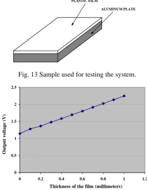
Fig. 13 Sample used for testing the system.
0 0.5 1 1.5 2 2.5 0 0.2 0.4 0.6 0.8 1 1.2
Thickness of the film (millimeters)
O u tp u t voltage (V)
Fig. 14 Output voltage plot dues to the different thickness of plastic coating on aluminum plate (0-1 mm). As we convert the lift-off into the thickness, the plot in fig. 14 shows the linearity of the measurement.
5. CONCLUSIONS
Our new designed eddy current system for measure the thickness of nonconductive coatings on nonferrous metal substrates has been detailed in the paper. Results of some preliminary experiments with coated aluminum plates has been shown satisfy sensitivities, linearity, resolution and stability of the system.
REFERENCES
[1] D. Kacprzak, T. Taniguchi, K. Nakamura, S. Yamada and M. Iwahara “ Novel Eddy Current Testing Sensor for the Inspection of Printed Circuit Boards” IEEE Trans. On Magnetics, Vol. 37, No. 4, July 2001, Page 2010-2012. [2] N.C. Haywood and J. R. Bowler. “Eddy-Current Imaging
of Buried Cracks by Inverting Field Data”. IEEE Trans. On Magnetics, Vol. 28, No.2, March 1992.
[3] John Hansen “The eddy current inspection method : Part 2.
The impedance plane and probes” Insight Vol 46 No 6 June 2004, page 364-365.
[4] Kofi D. Anim-Appiah and Sedki M. Riad. “Analysis and Design of Ferrite Cores for Eddy-Current-Killed Oscillator Inductive Proximity Sensors IEEE Trans. On Magnetics, Vol. 33, No. 3, May 1997.
[5] Prof. Moustafa N., I. Fahmy, Dr. Essam A. Hashish, Dr. Ibrahim Elshafiey and Dr. Ismael Jannoud. “Advanced System For Automating Eddy-Current Nondestructive Evaluation”. Seventeenth National Radio Science Conference, Minufiya University–Egypt. 22-24 Feb. 22-24,2000.