Electrical Conduction and Resistance Switching Mechanisms of Ag/ZnO/Ti Structure
Trung Do Nguyen*, Kim Ngoc Pham*, Vinh Cao Tran**, Duy Anh TuanNguyen***
and Bach Thang Phan*,**,★
Abstract
We investigated electrical conduction and resistance switching behavior of the Ag/ZnO/Ti structures for random access memory devices. These films were prepared on glass substrate by dc sputtering technique at room temperature. The resistance switching follows unipolar switching mode with small switching voltages (0.4 V – 0.6 V). Two electrical conduction mechanisms dominating the LRS and HRS are Ohmic and trap-controlled space charge limited current, respectively. These both conductions are consistent with the filamentary model. Based on the filamentary model, the switching mechanism was also interpreted.
Keywords: Resistance switching, random access memory, sputtering, ZnO thin films, filamentary model
*Faculty of Materials Science, University of Science, VNU-HCM, Vietnam
**Laboratory of Advanced Materials, University of Science, VNU-HCM, Vietnam
***Dong Nai University, Vietnam
★ Corresponding author: [email protected] Tel. +84 121 790 7700
※ Acknowledgment : This work is funded by National Foundation of Science and Technology Development of Vietnam (NAFOSTED – 103.99-2010.12)
Manuscript received May. 13, 2013; revised July. 1, 2013 ; accepted July 1. 2013
Ⅰ. Introduction
Resistance random access memory (ReRAM) has attracted extensive attention for their applications to nonvolatile data storage technologies due to its simple structure, low power consumption, low cost, nonvolality and high speed performance [1-12]. The resistance switching was observed from various materials, such as perovskite oxides (Pr0.7Ca0.3MnO3, La0.7Ca0.3MnO3, Cr-dopedSrZrO3, Cr-dopedSrTiO3…) [1-9], transition metal oxides (NiO, Ti, CuO, ZrO2,ZnO…)…[10-12]. The resistance switching effect is regarded as memory effect. The memory effect can be observed from the current – voltage
characteristics of metal – insulator – metal structure (MIM), in which resistance of the MIM structure reversely changes between the high resistance state (HRS) and the low resistance state (LRS), corresponding to logic signal (off and on state or 0 and 1 states). Two switching modes, unipolar switching and bipolar switching, have been observed to describe the switching between HRS and LRS.
Although the resistance switching effect can be obtained in various materials, the origin of resistance switching is controversial. The clear explanation of resistance switching in various materials is the challenge and motivation for current research.
We have already published our research on the resistance switching effect in Pt / Cr-doped SrTiO3 / La0.5Sr0.5CoO3structure[5-9]. Currently,we are investigating the resistance switching of binary oxides. In this study, we reported the electrical conduction and the resistance switching behavior of the Ag/ZnO/Ti structure.
Ⅱ. EXPERIMENTS AND DISCUSSION
The Ag/ZnO/Ti structure, as shown in Figure 1, was fabricated by sputtering technique at room temperature, ZnO thin film was sandwiched between
top (Ag) and bottom (Ti) electrode materials. A 150 nm-thick metallic Ti layer was deposited on a commercial glass substrate in Ar gas ambient of 6x10⁻³Torr, depositing current ITi=1A, while the 100nm-thick ZnO layer was deposited in Ar + O2(Ar/O2=1) mixed gas ambient of 6x10⁻³Torr, depositing current IZnO=0.3A. The Ag top electrode of 75 nm-thick was deposited on the ZnO thin film in Ar gas ambient of 6x10⁻³Torr, depositing current IAg=0.15A. During the deposition of Ag layer, a mask was used for top electrode patterning. The size of Ag top electrode is 1 mm in diameter.
Current-voltage (I-V) measurements were carried out using a Keithley 2400 source meter. During the electrical measurement, the positive sweep voltage is applied to the Ag top electrode, while the Ti bottom electrode is grounded. The thickness of these films were determined by Dektak 6M Stylus Surface Profilometer.
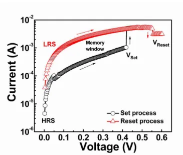
Figure 1: Schematic diagram of the Ag/ZnO/Ti structure As-prepared Ag/ZnO/Ti structures were initially in a high resistance state (HRS). To find out the switching voltages, we applied the 0 to Vmaxsweeping(Vmax = 0.1 V, 0.15 V, 0.2 V…) to observe the set process. Compliance current of 100 mA was applied to prevent permanent structure breakdown. In the 0 to 0.45 V sweeping (Vmax=0.45V), as shown in Figure 2, a sudden current increase (resistance decrease) from HRS to
low resistance state (LRS), was observed at about VSET~0.42V, the LRS remained until the end of the sweeping. This sweeping switched the structure into LRS, corresponding to “set” process.
Figure 2: I-V characteristics of the Ag/ZnO/Ti structure The Ag/ZnO/Ti structure now is in LRS. The next sweeping process from 0 to Vmax(0.1V,0.15V,0.2V….) was applied to the structure to observe the reset process. The I-V characteristics in this process is different from that in the set process above (0 to 0.45 V), as shown in red color. The value of current of the reset process is higher than the current value of the set process measured at the same voltage. In the 0 to 0.6 V sweeping process, current increased linearly with sweeping voltage until 0.51 V, then current gradually decreased. An abrupt drop of current could be observed at voltage of 0.55 V (VRESET~0.55V), the structure switched back to HRS.
The set and reset process correspond to the “write”
and “erase” data in storage device. We can observe the memory effect or memory window (two current values at a certain voltage) in the voltages below VSET. The I-V curve with a triangle shape is visible, similar to the model of memristive system analyzed by Strukov etal[13]. The resistance switching is in unipolar mode, the switching between HRS and LRS only depends on magnitude of sweeping voltage, not polarity. In the following sweepings, the unipolar
resistance switching could be observed repeatedly.
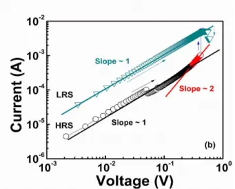
Figure 3: I-V characteristics of HRS in log-log scale
In order to understand the electrical conduction and switching mechanisms of the memory devices, the typical I-V characteristics of Ag/ZnO/Ti structure were plotted in log-log scale. The workfunctions of Ti and Ag are about 4.2 - 4.5 eV, the electron affinity of ZnO is about 4.5 eV. As shown in Fig. 3, the current of the HRS significantly varies with voltage. To see the variation visibly, the current data in different voltage regions were plotted in different colours. The fitting data showed that the leakage current at a lowest voltage region (0 – 0.3 V, in black colour) depicts a linear dependence on voltage (slope ~ 1), this linear dependence is a typical behavior of a Ohmic conduction [5,13,14]. In the higher voltage regions (0.3 – 0.42 V, in red colour), the nonlinear I-V characteristic appears. The classical nonlinear conduction mechanisms including Schottky emission, Poole-Frenkel emission and trap-controlled space charge limited conduction were adpoted to fit the nonlinear I-V curve. It was found that the trap-controlled space charge limited current has the best fit. The current shows a square term dependence on voltage (slope ~ 2), which is the typical characteristics of a trap-controlled space charge limitted current conduction [5,9,13-15]. The HRS to LRS switching occurs at about 0.42 V and then the current in the highest voltage region (0.42 - 0.45 V, in blue) follows the linearly Ohmic behavior (slope ~ 1). The electrical conduction of the LRS can
be defined in Fig. 4. The current of LRS (in dark cyan colour) varies linearlity with voltage in a wide voltage ranges (0 – 0.55 V) with a slope of 1. This might describe the carrier transport though the conducting paths.
Figure 4: I-V characteristics of LRS and HRS in log-log scale
The linearly behavior of the LRS and the square term dependence of the HRS are the markers for understanding the switching mechanism. The resistance switching mechanism can be explained via filamentary model [16]. In filamentary model, defects are almost the key factors. The structural defects are oxygen vacancies, metallic defects… are inevitable, which act as trap centers for charge carriers [7,12].
In the set process, the current transport through the oxide films via trap-controlled space charge limited (SCLC) conduction and the defects align to form tiny conducting filaments. In high voltage regions, these tiny conducting filaments gather together to form stronger and more conducting filaments. In addition, the injected carriers are dominant and are captured by traps, resulting in SCLC. The both processes reduce the structural resistivity and the HRS switches to the LRS at 0.42 V. Above the set voltage (VSET=0.42V), the carriers transport through the filament paths, corresponding to the Ohmic conduction. In the reset process, the carriers still transport through the filament paths. At reset voltage (VRESET=0.52V), the filament paths are ruptured by Joule heating effect since the large injected carrier density flows through the filament paths, the LRS switches back to the HRS . These our explainations
are consistent to the published data in other ZnO-based structures [12,15]. In addition, we also prepared the ZnO films at different pressures of 10-2Torr, 6x10⁻³Torr and 2x10⁻³Torr. Among these films, the films deposited at the low pressures (6x10⁻³Torr and 2x10⁻³Torr) showed the resistance switching, while the ZnO films deposited at the high pressure of 10-2Torr did not show the resistance switching. Therefore, the defect involved in the resistance switching in the filamentary model is oxygen vacancies. This content will be published elsewhere.
Ⅲ. CONCLUSION
The Ag/ZnO/Ti structures were prepared on glass substrate by dc sputtering technique. The resistance switching behavior of the Ag/ZnO/Ti structure was demonstrated. The resistance switching follows unipolar switching mode. The conduction mechanism dominating the LRS and HRS are Ohmic and trap-controlled space charge limited current, respectively. These both conductions are consistent with the filamentary model and the switching mechanism was interpreted.
References
[1] C. Rossel, G.I. Meijer, D. Bremaud and D.
Widmer, J. Appl. Phys. 90,2892(2001)
[2] G. Meijer, I.U. Staub, M. Janousch, S.L. Johnson, B. Delley and T. Neisius, Phys. Rev. B 72,155102(2005)
[3] A. Odagawa, H. Sato, I.H. Inoue, H. Akoh, H.
Kawasaki, M.Y. Tokura, T. Kanno and H. Adachi, Phys. Rev. B 70,224403(2004)
[4] A. Sawa, T. Fujii, M. Kawasaki and Y. Tokura, Appl. Phys. Lett. 88,232112(2006)
[5] B. T. Phan, T. Choi, and J. Lee, J. Korean Phys.
Soc. 51,664(2007).
[6] B. T. Phan, T. Choi, and J. Lee, Integrated Ferroelectrics 96,146(2008).
[7] B. T. Phan and J. Lee, Appl. Phys. Lett.
93,222906(2008).
[8] B. T. Phan, N. C. Kim, and J. Lee, J. Korean Phys. Soc. 54,873(2009).
[9] B. T. Phan and J. Lee, Appl. Phys. Lett.
94,232102(2009).
[10] Shibing Long, Qi Liu, Hangbing Lv, Yingtao Li, YanWang, Sen Zhang, Wentai Lian, Kangwei Zhang, MingWang, Hongwei Xie, Ming Liu, Appl. Phys. A.
102,915(2011).
[11] Young Ho Do, June Sik Kwak and Jin Pyo Hong, Hyunsik Im, Bae Ho Park, J. Korean Phys.
Soc. 5,1009(2009).
[12] Xinman Chen, Guangheng Wu, and Dinghua Bao, Appl. Phys. Lett. 93,093501(2008).
[13] D. B. Strukov, G. S. Snider, D. R. Stewart, and R. S. Williams, Nature (London). 453,80(2008).
[14] K. C. Kao and W. Huang,
ElectricalTransportinSolid (Pergamon, Oxford, U.K), (1981).
[15] Lei Shi, Dashan Shang, Jirong Sun and Baogen Shen, Appl. Phys. Exp 2,101602(2009).
[16] B. J. Choi, D. S. Jeong, S. K. Kim, C. Rohde, S.
Choi, J. H. Oh, H. J. Kim, C. S Hwang, K. Szot, R.
Waser, B. Reichenberg, and S. Tiedke, J. Appl. Phys.
98,033715(2005).
BIOGRAPHY
Trung Do Nguyen
2009: BS degree in Physics, University of Science, Vietnam National University, HoChiMinh City, Vietnam.
<Main interesting field> Memory devices.
Kim Ngoc Pham
2006: BS degree in Materials Science, University of Science, Vietnam National University, HoChiMinh City, Vietnam.
2011: MS degree in Electronic Physics, University of Science, Vietnam National University, HoChiMinh City, Vietnam.
<Main interesting field> Electronic materials, Memory devices.
Cao Vinh Tran
Name: 1994: BS degree in Physics, University of Science, Vietnam National University, HoChiMinh City, Vietnam.
1998: MS degree in Optical Physics, University of Science, Vietnam National University, HoChiMinh City, Vietnam.
2009: PhD in degree in Optical Physics, University of Science, Vietnam National University,
HoChiMinh City, Vietnam
<Main interesting field> Transparent conducting oxides, Memory devices.
Nguyen Duy Anh Tuan
1986: BS degree in Physics at University of Pedagogy Ho Chi Minh City.
2000: MS degree in Electronics at University of Science Ho Chi Minh City
2009: PhD in solid State Physics at University of Science Hue City
<Main interesting field> Materials Science
Bach Thang Phan
2001: BS degree in Physics, University of Science, Vietnam National University, HoChiMinh City, Vietnam.
2009: PhD degree in Advanced Materials Science and
Engineering, SungKyunKwan University, South Korea.
<Main interesting field> Electronic materials, Magnetic materials, Memory devices.