Review http://dx.doi.org/10.14478/ace.2015.1077
유기 전기 발광소자의 원리와 연구동향
신환규⋅김승호⋅이재현⋅이하윤⋅정효철⋅박종욱†
가톨릭대학교 화학과 (2015년 7월 9일 접수)
Research Trends in Organic Light Emitting Diode
Hwangyu Shin, Seungho Kim, Jaehyun Lee, Hayoon Lee, Hyocheol Jung, and Jongwook Park†
Department of Chemistry, Catholic University of Korea, 43 Jibongro, Wonmigu, Bucheonsi, Gyenggido 420-743, Republic of Korea (Received July 9, 2015)
초 록
유기 발광 다이오드(OLED)는 학문 및 산업분야에서 많은 관심을 받아 왔으며, 소자가 갖는 우수한 장점을 바탕으로 모바일 디스플레이뿐만 아니라 대면적 TV, 차세대 굴곡형 디스플레이의 적용이 활발하게 진행되고 있다. 또한 OLED 재료의 연구와 소자제작 기술의 응용 연구 범위를 넓혀가고 있다. 본 논문에서는 이러한 OLED에 대한 기본적인 소자 구성 및 원리를 설명하고, 다양한 화학구조를 응용한 OLED 재료를 각각의 용도에 맞게 분류 정리하였다. 이러한 OLED 기술의 개념과 재료의 특성을 체계적으로 분류함으로써 새로운 발광 재료를 연구하고 개발함에 있어서 많은 도움이 되리라고 생각한다.
Abstract
Organic Light Emitting Diodes (OLEDs) have been receiving great attention in academic and industrial fields, and it is being actively applied to mobile display, as well as large area TV and next-generation flexible display due to their excellent advantages. In addition, the scope of research on OLED materials and device fabrication technology is getting expanded. This review discusses the principle and basic composition of OLED and also classifies OLED materials with different chemical structures according to their usages. Systematic classification of OLEDs by technical concept and material characteristics can help developing new emitting materials.
Keywords: organic light emitting diode, fluorescence, phosphorescence, hole transporting layer, electron transporting layer
1. Introduction
1)There are many research fields in which Korea needs to show scien- tific development, but representative next-generation research fields in- clude semiconductor, energy storage device and display. Organic Light Emitting Diode (OLED) technology, rising as the core technology of display field among such three major fields, has recently replaced LCD and PDP on TV application. It is widely used in small and medium sized devices such as smart phone and MP3 player. Many studies are being conducted on TV and lighting applications to make use of ad- vantages of OLEDs such as flexibility, self emission, full color emis- sion, low driving voltage and fast response time[1-4]. This paper re- ports the basic principle of organic materials and related technology applied to OLEDs, which are considered as extremely important for the
† Corresponding Author: Department of Chemistry, Catholic University of Korea, 43 Jibongro, Wonmigu, Bucheonsi, Gyenggido 420-743, Republic of Korea Tel: +82-2-2164-4821 e-mail: [email protected]
pISSN: 1225-0112 eISSN: 2288-4505 @ 2014 The Korean Society of Industrial and Engineering Chemistry. All rights reserved.
development of next generation display.
As shown in Figure 1, OLEDs have an organic semiconductor in- serted between two electrodes as thin film of 10 nm~100 nm thickness. When electricity is supplied, electron and hole are injected through cathode (metal electrode, Al is commonly used) and anode (ITO is commonly used). The injected electron passes through electron injection layer and electron transport layer, and the injected hole passes through hole injection layer and hole transport layer. They encounter in emitting layer and recombine to form exciton. Electric energy of this exciton is converted into light energy. Here, light is embodied with a color that corresponds to energy band gap of the compounds which constitute the emitting layer. Most of thin film materials are organic compounds and organometallic compounds (see Figure 2(a)).
Organic semiconductor materials can be explained using basic char- acteristic terms as follows. Organic semiconductor materials consist of organic compounds that include carbon and other atoms based on shar- ing electrons. They form molecules through covalent bonding, and atomic orbital (AO) is transformed into molecular orbital (MO). Here, MO has two pairs of AOs which participate to form bonding orbital
Glass ITO(Indium Tin Oxide)
(+)
EML(Emitting Layer) Metal (-)
HIL(Hole Injection Layer) HTL(Hole Transporting Layer)
ETL(Electron Transporting Layer) EIL(Electron Injection Layer)
Glass ITO(Indium Tin Oxide)
(+)
EML(Emitting Layer) Metal (-)
HIL(Hole Injection Layer)
HIL(Hole Injection Layer) HTL(Hole Transporting Layer)HTL(Hole Transporting Layer) ETL(Electron Transporting Layer) ETL(Electron Transporting Layer) EIL(Electron Injection Layer)
EIL(Electron Injection Layer)
Figure 1. Basic structure of OLED device.
(a)
Homo Lumo
Valence Band Conduction Band
Homo Lumo
Valence Band Conduction Band
(b) Figure 2. (a) Performance property of OLEDs device, (b) Band gap of organic semiconductor.
and antibonding orbital. Many bonding orbitals gather to create a band, and this band is referred to as valence band. Then band of antibonding orbitals is called conduction band. Highest energy level of the valence band is called highest occupied molecular orbital (HOMO), and lowest energy level of the conduction band is called lowest unoccupied molec- ular orbital (LUMO) (see Figure 2(b)). The energy difference between HOMO and LUMO is referred to as band gap. Since metals do not have band gap, electrons can freely move between the valence band and conduction band to show electric conductivity and thermal conductivity. On the contrary, nonconductors have large band gap, which causes great difficulty for electrons to move from the valence band to the conduction band. Organic semiconductor materials have in- termediate band gap among organic compounds which belongs to sem- iconductor domain, showing similar characteristics as inorganic semi- conductor materials. In general, organic compounds include conjugated double bond having alternating double and single bonds. As a result, many organic compounds contain ring components such as benzene ring. Colors of red, green and blue and color purity are determined based on band gap of such organic semiconductor emitting materials, and materials generally have band gap of 2.0 eV~4.0 eV. Here, 2.75 eV corresponds to blue light with wavelength of 450 nm. 2.4 eV corre- sponds to green light with wavelength of 510 nm, and 2 eV corre- sponds to red light with wavelength of 620 nm. Also, thin film of or- ganic semiconductor materials are mostly deposited by vacuum deposi- tion method using organic compound or organometallic compound.
Spin coating, ink-jet and laser induced thermal imaging (LITI) were re- cently used to fabricate devices for diversity of preparation process and broader application.
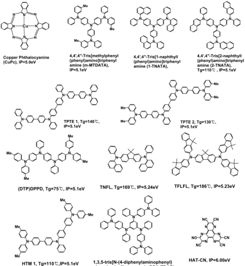
2. Hole Injection Layer (HIL)
Composition of each layer shown in Figure 1 is as follows. Indium tin oxide (ITO) glass, an inorganic oxide, forms a substrate as trans- parent electrode. Hole injection layer is placed on top of this substrate.
Hole injection layer is also known as buffer layer, and the two terms are used to mean the same. On the ITO surface, hole injection into or- ganic layer has energy barrier, so HOMO level of HIL should be lo- cated between ITO and hole transport layer (HTL). Since inorganic and organic substances have different surface energy, buffer materials should have medium surface energy value. Materials used in hole in- jection layer also have thermal stability with glass transition temper- ature (Tg) of 90 ℃ or above. Furthermore, since ITO has rough and non-flat surface, hole injection layer is coated on top of ITO to soften its surface. This layer is designed to have intermediate HOMO value between work function of ITO and HOMO level of hole transport layer in order to fit and adjust the difference between work function of ITO and HOMO level of hole transport layer (see Figure 2). In addition, hole injection layer also requires appropriate hole conductivity.
Characteristics of hole injection layer are briefly summarized below (see Figure 3).
- Efficient hole injection from anode to emitting layer
- Intermediate energy level and high band gap energy of anode and hole transport
- High band gap energy for electron blocking - Formation of non-crystalline thin film - High thermal stability
- Good adhesion with ITO and flat surface
N N
N N Me
Me
Me
N N
N N
N N
N N
4,4′,4′′-Tris[methylphenyl (phenyl)amino]triphenyl amine (m-MTDATA), IP=5.1eV
4,4′,4′′-Tris[1-naphthyll (phenyl)amino]triphenyl amine (1-TNATA),
4,4′,4′′-Tris[2-naphthyll (phenyl)amino]triphenyl amine (2-TNATA), Tg=110℃ , IP=5.1eV Cu
N
N N
N
N N
N N
Copper Phthalocyanine (CuPc), IP=5.0eV
N N
N N
TPTE 1, Tg=140℃, IP=5.1eV
N N
N N
Me
Me
Me Me
TPTE 2, Tg=130℃, IP=5.1eV
N Me
Me N
N N Me
Me
(DTP)DPPD, Tg=75℃, IP=5.1eV
N N
TNFL, Tg=169℃, IP=5.24eV
N N
TFLFL, Tg=186℃, IP=5.23eV
N N
N Me
Me
Me Me
HTM 1, Tg=110℃,IP=5.1eV
N N
N N
N
N
1,3,5-tris[N-(4-diphenylaminophenyl) phenylamino]benzene, (p-DPA-TDAB)
N N N
N N
N NC CN
NC
NC CN
CN
HAT-CN, IP=6.00eV
Figure 3. Examples of hole injection materials.
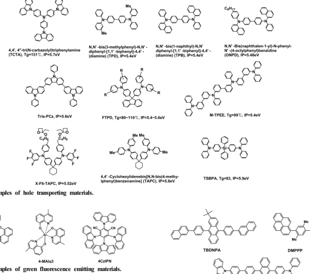
3. Hole Transport Layer (HTL)
The role of hole transport layer is to stably provide hole that comes in through hole injection layer to emitting layer. HOMO level of hole transport layer is also higher than HOMO level of emitting layer for smooth hole transport. Here, hole mobility of hole transport layer acts as an important factor of performance improvement in devices in re- gards to thickness of thin film because of charge balancing effect (the effect in which high electroluminescence (EL) efficiency can be ob- tained when similar number of holes and electrons is injected into emitting layer). Since material of hole transport layer must have high hole mobility and it contacts emitting layer, it is extremely important for the HOMO level value to be between hole injection layer and emit- ting layer in order to suppress generation of exciton on hole transport layer - emitting layer interface. Also, hole transport layer is required to have an ability to appropriately control electrons transported from emitting layer. Therefore, layer with smaller electron affinity, which means large band gap, has excellent characteristics. Materials of hole transport layer generally include electron donor moiety and can be re- garded as p-type of semiconductor, mainly consisting of aromatic
amines (see Figure 4). Characteristics of hole transport layer can be briefly summarized as follows[5-8].
- High hole mobility
- HOMO level between hole injection layer and emitting layer - Low LUMO value for electron blocking
- Non-crystalline thin film - High thermal stability - High band gap energy
4. Emitting Materials - Fluorescent Materials
Materials of emitting layer are largely divided into fluorescent emit- ting materials and phosphorescent emitting materials, and they are fur- ther classified according to color. Holes injected from HTL and elec- trons injected from ETL form exciton in emitting layer to emit light.
Color purity and emission efficiency are reduced by molecular interac- tion when only an emitting material is used, and this is why host/dop- ant system is widely used. This system is used to minimize interaction of emitting dopant distributed in the host and to increase emission effi- ciency through energy transfer. Holes and electrons excite the host, and
N
N N N
N Me
N Me
N N
N N
Me
Me Me
Me
N N
N N
N N
C8H17
N N
F F
F
F F
F C4H8 C4H8
O O
O O
N
N N
N N
R R R
R
Si
N N
4,4', 4"-tri(N-carbazolyl)triphenylamine (TCTA), Tg=151℃, IP=5.7eV
N,N' -bis(3-methylphenyl)-N,N' - diphenyl-[1,1' -biphenyl]-4,4' - (diamine) (TPD), IP=5.4eV
N,N' -bis(1-naphthyl)-N,N' diphenyl-[1,1' -biphenyl]-4,4' - (diamine) (TPB), IP=5.4eV
4,4' -Cyclohexylidenebis[N,N-bis(4-methy- lphenyl)benzenamine] (TAPC), IP=5.8eV
M-TPEE, Tg=98℃, IP=5.4eV
N,N' -Bis(naphthalen-1-yl)-N-phenyl- N' -(4-octylphenyl)benzidine (ONPD), IP=5.48eV
X-F6-TAPC, IP=5.52eV
Tris-PCz, IP=5.6eV FTPD, Tg=80~110℃, IP=5.4~5.6eV
TSBPA, Tg=83, IP=5.9eV
Figure 4. Examples of hole transporting materials.
N O
Al
N O
N O
N O
Al
N O
N O
N
NC CN
N N
N
Alq3 4-MAlq3 4CzIPN
Figure 5. Examples of green fluorescence emitting materials.
Me
Me
TBDNPA DMPPP
N N
BN2
Figure 6. Examples of blue fluorescence emitting materials.
the dopant absorbs excitation energy and reemits energy to release light. Ideally, emission spectrum of the host should be identical to ab- sorption spectrum of the dopant for smooth energy transfer from the host to the dopant, but energy transfer is known to be able to occur well when only 1/3 of the spectra overlaps. Thus, a dopant with desir- able emission wavelength and a host that can sufficiently transfer en- ergy must be combined to embody excellent color.
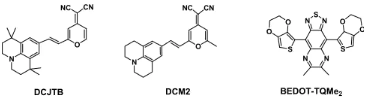
4.1. Green Emitting Materials
Alq3, a green emitting material, is the very first emitting material developed among emitting materials currently in use. Alq3 was first used in OLED by Kodak in 1987. It is not only used as green emitting material but also as host of red emitting material and ETL material in passive OLED device. Among many derivatives based on Alq3, 4-MAlq3 which has methyl oup at 4-position is known to have high emission efficiency. Many green emitting materials with high quantum efficiency have recently been reported and developed using thermally activated delayed fluorescence (TADF)[9](see Figure 5).
4.2. Blue Emitting Materials
Derivatives with high fluorescent quantum efficiency and wide band gap such as anthracene, pyrene, carbazole and fluorene are mainly used
as blue emitting materials[10-12]. Since blue emitting materials have wide band gap, they require greater voltage for injection of holes and ectrons from nearby electron and hole transport layers to emitting layer.
This causes problems of reduced lifetime and efficiency in device operation. They fail to secure sufficient lifetime due to relatively inferior properties of color purity, efficiency and thermal stability compared to other colors. As materials used in commercialized products are ex- tremely limited, further research and development efforts are needed.
Moreover, blue emission wavelength band required in mid and large sized TV is shorter (450 nm or below) than wavelength band of existing materials, it is very urgent to develop materials with desirable emission wavelength, high efficiency and long lifetime of device (see Figure 6).
4.3. Red Emitting Materials
Many red emitting materials were reported by Kodak of the United States and Mitsubishi Chemical and Sony of Japan in case of passive OLED device. Among them, DCJTB of Kodak is the representative emitting material. DCJTB as dopants is known to exhibit improved emission efficiency when rubrene host, a yellow emitting material, is
O CN NC
N
DCM2 N
O NC CN
DCJTB
N N
SN N
S S
O
O O O
BEDOT-TQMe2
Figure 7. Examples of red fluorescence emitting materials.
Figure 8. Examples of yellow and orange fluorescence emitting materials.
N N
N PtN
PtOEP
Figure 9. Example of Pt type phosphorescence emitting materials.
Ir N
N F
R
R
N F
O O F
F
Firpic (R=H) m-Firpic (R=CH3) N-Firpic (R=NMe2)
Figure 10. Examples of blue phosphorescence materials based on fluorine.
used. However, its emission wavelength is less than 650 nm, and color purity and emission efficiency are reduced by broad emission area.
Materials that emit light in the near-IR region based on conjugated struc- ture of donor-acceptor-donor were recently reported[13](see Figure 7).
4.4. Yellow and Orange Emitting Materials
As shown in Figure 8, rubrene and BTX are representative yellow and orange emitting materials. Displays and lighting applications in general can embody colors of all wavelengths by mixing three primary colors of red, green and blue, but mixing of three primary colors re- sults in a color close to white with reduced chromaticity. Perfect color can be embodied using emitting materials that exhibit wavelengths of yellow and orange colors.
5. Emitting Materials - Phosphorescent Materials
When electrons in a molecule receive energy to become excited, they either exist in singlet state or triplet state. They have 25% chance of being in singlet state and 75% chance of being in triplet state.
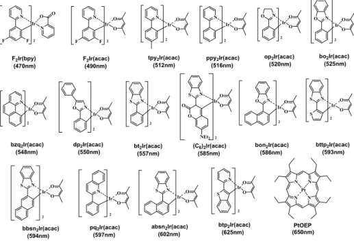
Fluorescent light emitted when electrons drop from singlet state to ground state, and phosphorescent light emitted when electrons drop from triplet state to ground state. Therefore, maximum internal quan- tum efficiency is 25% for fluorescent light and 75% for phosphor- escent light. When electrons can be transferred from triplet state to ex- cited singlet state, 100% internal quantum efficiency can theoretically be achieved. However, electron transfer from triplet state to ground state based on the selection rule is prohibited in light emission. When the core metal is heavy (e.g. iridium (Ir), platinum (Pt), europium (Eu), terbium (Tb), ruthenium (Ru) and osmium (Os)), light emission is available by spin-orbit coupling. Phosphorescent emitting materials are materials that have increased emission efficiency based on this princi- ple[14-17].
Professor M. E. Thompson and professor S. Forrest were the first to develop a red phosphorescent emitting material named PtOEP, which used platinum as core metal mixed with organic ligand, when they worked at Princeton University in 1999 (see Figure 9). This material had high thermal stability and excellent color purity because of narrow emis
sion area, but long existence in triplet state causes triplet-triplet annihila- tion when high current density is applied. Efficiency and luminance were reduced during device operation[18]. They conducted a joint re- search to develop and report an iridium phosphorescent emitting material called Ir(ppy)3. Ir(ppy)3 showed high emission efficiency (40 lm/W or above) and has recently been used in many studies with various phos- phorescent hosts[19].
Especially, universal display company (UDC) jointly developed a blue emitting material named FIrpic in 2001. FIrpic is being actively studied as a representative blue phosphorescent material with diverse applications. Despite its high emission efficiency, it cannot be seen as perfect blue in terms of color purity[20]. Accordingly, different de- rivatives were developed in order to replace FIrpic as representative phosphorescent blue emitting material. In 2013, professor Kim et al. de- veloped a blue phosphorescent material in the deep blue region called (TF)2Ir(fptz) and reported color coordinates of (0.147, 0.116) to present possibility of osphorescent materials with deep blue wavelength[21]
(see Figure 10). Other phosphorescent materials are shown in Figure 11.
Figure 11 shows main ligand and ancillary ligand, and their effects are as follows. The main ligand decides color. Color moves to the blue region as electron density of nitrogen increases, and it moves to the blue region when the ligand becomes bulkier. Also, the ancillary ligand affects subtle color tunning and has a tendency to move to the blue region when conjugation is small (see Figure 12).
6. Electron Injection Layer and Electron Transport Layer
Electron injection layer is inserted between cathode and electron transport layer. It is used for smooth injection of electrons. Metal ions such as LiF and CsF are mainly used for electron injection layer.
Electron transport layer is generally a material that includes compo nents to withdraw electrons. And it must stably provide electrons to
F2Ir(bpy) (470nm)
F2Ir(acac) (490nm)
tpy2Ir(acac) (512nm)
ppy2Ir(acac) (516nm)
op2Ir(acac) (520nm)
O N
IrO O
2 N
Ir O O
2 N
Ir O O
2 N
Ir O O
2 N
Ir N O
2 O
F F
F F
O N
IrO O
2
bon2Ir(acac) (586nm) S N
O IrO
O O
NEt2 2
(C6)2Ir(acac) (585nm) S N
IrO O
2
bt2Ir(acac) (557nm) O N
IrO O
2
dp2Ir(acac) (550nm) N
IrO O
2
bzq2Ir(acac) (548nm)
O N IrO
O
2
bo2Ir(acac) (525nm)
S N Ir O
O
2
bbsn2Ir(acac) (594nm)
S N Ir O
O
bttp2Ir(acac) (593nm)
S 2
N Ir O
O
2
pq2Ir(acac) (597nm)
S N Ir O
O
2
absn2Ir(acac) (602nm)
N
S IrO
O
2
btp2Ir(acac) (625nm)
N N
N N
Pt
PtOEP (650nm)
Figure 11. Examples of phosphorescence materials based on metal-ligand complex.
Figure 12. Diagram of phosphorescence materials based on metal-ligand complex.
N N N
N N N
N N
TPBi Bphen
N
N N O
O O
Al
Alq3
Figure 13. Examples of typical electron transporting materials.
Figure 14. Examples of electron transporting materials.
Figure 15. Examples of electron transporting materials based on molecular orientation.
emitting layer by smoothly transporting electrons based on high elec- tron mobility. It also requires appropriate LUMO value compared to electron injection layer and low HOMO value to block holes. Figure
13 shows representative materials used as electron transport layer.
Contrary to hole transport layer, materials of electron transport layer correspond to n-type of semiconductor and introduce a chemical group that can withdraw electrons. Since strong withdrawing effect of elec- trons can result in quenching, it is important to increase electron mobi- lity using appropriate electron withdrawing moiety. Pyridine and ox- adiazole are representative groups[22-24] (see Figure 14). Recent stud- ies also report increasing effect of electron mobility using molecular orientation[25,26] (see Figure 15).
7. Conclusion
OLED display panels have many advantages compared to LCD pan- els such as relatively simple composition of panel with lack of re- tardation film, single polarizer, no alignment layer and no color filter.
And OLED has excellent characteristics like high luminance, self emis- sion, high color purity, high contrast, low power consumption, ex- cellent viewing angle, and slim design. In comparison to other dis- plays, OLED has relatively short time for development and fails to achieve high performance and large size display panels.
Such internal tasks can be resolved through development of element technologies. Research efforts on these technologies are urgently de- manded, but comparing on simple panel structure as an advantage, ma- terial layers in OLEDs are playing the role of several layers in LCD.
In other words, competitiveness of internal materials in OLEDs is directly led to competitiveness of OLED panels. Considering the fact that OLED technologies are being actively developed, development of internal materials in OLEDs must have priority as the focus of research.
Acknowledgement
This research was supported by a grant from the Fundamental R&D Program for Core Technology of Materials funded by the Ministry of Trade, Industry and Energy, Republic of Korea (Project No. 10050215).
References
1. Z. Shen, P. E. Burrows, V. Bulović, S. R. Forrest, and M. E.
Thompson, Three-color, tunable, organic light-emitting devices, Science, 276, 2009-2011 (1997).
2. S. R. Forrest, The road to high efficiency organic light emitting devices, Org. Electron., 4, 45-48 (2003).
3. A. R. Duggal, J. J. Shiang, C. M. Heller, and D. F. Foust, Organic light-emitting devices for illumination quality white light, Appl.
Phys. Lett., 80, 3470-3472 (2002).
4. B. W. D’Andrade and S. R. Forrest, White organic light-emitting devices for solid-state lighting, Adv. Mater., 16, 1585-1595 (2004).
5. L. S. Cui, S. C. Dong, Y. Liu, Q. Li, Z. Q. Jiang, and L. S. Liao, A simple systematic design of phenylcarbazole derivatives for host materials to high-efficiency phosphorescent organic light-emitting diodes, J. Mater. Chem. C., 1, 3967-3975 (2013).
6. S. Inayama, N. Takahashi, Y. J. Pu, T. Chiba, H. Sasabe, and J.
Kido, Syntheses of solution-processable arylamine derivatives and their application to organic light emitting devices, J. Photopolym.
Sci. Techol., 25, 335-339 (2012).
7. G. Liaptsis and K. Meerholz, Crosslinkable TAPC-based hole-transport materials for solution-processed organic light-emit- ting diodes with reduced efficiency roll-off, Adv. Funct. Mater., 23, 359-365 (2013).
8. C. W. Lee and J. Y. Lee, Low driving voltage and high power ef- ficiency in blue phosphorescent organic light-emitting diodes using aromatic amine derivatives with diphenylsilyl linkage, Synthetic Metals., 167, 1-4 (2013).
9. H. Uoyama, K. Goushi,K. Shizu, H. Nomura, and C. Adachi, Highly efficient organic light-emitting diodes from delayed fluo- rescence, Nature, 492, 234-240 (2012).
10. C. J. Zheng, W. M. Zhao, Z. Q. Wang, D. Huang, J. Ye, X. M.
Ou, X. H. Zhang, C. S. Lee, and S. T. Lee, Highly efficient non-doped deep-blue organic light-emitting diodes based on an-
thracene derivatives, J. Mater. Chem., 20, 1560-1566 (2010).
11. K. C. Wu, P. J. Ku, C. S. Lin, H. T. Shih, F. I. Wu, M. J. Huang, J. J. Lin, I. C. Chen, and C. H. Cheng, The photophysical proper- ties of dipyrenylbenzenes and their application as exceedingly effi- cient blue emitters for electroluminescent devices, Adv. Funct.
Mater., 18, 67-75 (2008).
12. B. Wei, J. Z. Liu, Y. Zhang, J. H. Zhang, H. N. Peng, H. L. Fan, Y. B. He, and X. C. Gao, Stable, glassy, and versatile binaph- thalene derivatives capable of efficient hole transport, hosting, and deep-blue light emission, Adv. Funct. Mater., 20, 2448-2458 (2010).
13. Y. Yang, R. T. Farley, T. T. Steckler, S. H. Eom, J. R. Reynolds, K. S. Schanze, and J. Xue, Efficient near-infrared organic light-emitting devices based on low-gap fluorescent oligomers, J.
Appl. Phys., 106, 044509-1-044509-7 (2009).
14. J. P. Duan, P. P. Sun, and C. H. Cheng, New Iridium complexes as highly efficient orange-red emitters in organic light-emitting di- odes, Adv. Mater., 15, 224-228 (2003).
15. C. Borek, K. Hanson, P. I. Djurovich, M. E. Thompson, K.
Aznavour, R. Bau, Y. Sun, S. R. Forrest, J. Brooks, L. Michalski, and J. Brown, Highly efficient, near-infrared electro phos -phorrescence from a Pt–metalloporphyrin complex, Angew.
Chem. Int. Ed., 119, 1127-1130 (2007).
16. Y. Tung, L. Chen, Y. Chi, P. Chou, Y. Cheng, E. Y. Li, G. H.
Lee, C. F. Shu, F. I. Wu, and A. J. Carty, Orange and red organic light-emitting devices employing neutral Ru(II) emitters: rational design and prospects for color tuning, Adv. Funct. Mater., 16, 1615-1626 (2006).
17. Y. L. Tung, P. C. Wu, C. S. Liu, Y. Chi, J. K. Yu, Y. H. Hu, P. T. Chou, S. M. Peng, G. H. Lee, Y. Tao, A. J. Carty, C. F.
Shu, and F. I. Wu, Highly efficient red phosphorescent osmium(II) complexes for OLED applications, Organometallics, 23, 3745-3748 (2004).
18. M. A. Baldo, D. F. O’Brien, Y. You, A. Shoustikov, S. Sibley, M.
E. Thompson, and S. R. Forrest, Highly efficient phosphorescent emission from organic electroluminescent devices, Nature, 395, 151-154 (1998).
19. M. A. Baldo, S. Lamansky, P. E. Burrows, M. E. Thompson, and S. R. Forrest, Very high-efficiency green organic light-emitting de- vices based on electrophosphorescence, Applied Physics Letters., 75, 4-6 (1999).
20. A. F. Rausch, M. E. Thompson, and H. Yersin, Matrix effects on the triplet state of the OLED emitter Ir(4,6-dFppy)2(pic) (FIrpic):
investigations by high-resolution optical spectroscopy, Inorganic Chemistry, 48, 1928-1937 (2009).
21. S. Lee, S. O. Kim, H. Shin, H. J. Yun, K. Yang, S. K. Kwon, J.
J. Kim, and Y. H. Kim, Deep-blue phosphorescence from per- fluoro carbonyl-substituted Iridium complexes, J. Am. Chem. Soc., 135, 14321-14328 (2013).
22. S. Oyston, C. Wang, G. Hughes, A. S. Batsanov, I. F. Perepichka, M. R. Bryce, J. H. Ahn, C. Pearson, and M. C. Petty, New 2,5-di- aryl-1,3,4-oxadiazole-fluorene hybrids as electron transporting ma- terials for blended-layer organic light emitting diodes, J. Mater.
Chem., 15, 194-203 (2005).
23. M. Ichikawa, T. Kawaguchi, K. Kobayashi, T. Miki, K. Furukawa, T. Koyama, and Y. Taniguchi, Bipyridyl oxadiazoles as efficient and durable electron-transporting and hole-blocking molecular ma- terials, J. Mater. Chem., 16, 221-225 (2006).
24. S. J. Su, D. Tanaka, Y. J. Li, H. Sasabe, T. Takeda, and J. Kido, Novel four-pyridylbenzene-armed biphenyls as electron-transport ma- terials for phosphorescent OLEDs, Org. Lett., 10, 941-944 (2008).
25. H. Sasabe, T. Chiba, S. J. Su, Y. J. Pu, K. I. Nakayama, and J.
Kido, 2-Phenylpyrimidine skeleton-based electron-transport materi- als for extremely efficient green organic light-emitting devices,
Chem. Commun., 5821-5823 (2008).
26. D. Yokoyama, H. Sasabe, Y. Furukawa, C. Adachi, and J. Kido, Molecular stacking induced by intermolecular C-H…N hydrogen bonds leading to high carrier mobility in vacuum-deposited organic films, Adv. Funct. Mater., 21, 1375-1382 (2011).