http://dx.doi.org/10.46670/JSST.2021.30.5.309 pISSN 1225-5475/eISSN 2093-7563
유기발광소자에 적용 가능한 NiO x 기반의 정공주입층 연구
김준모1,2 · 김예진1,2 · 이원호1,2,+ · 이동구3,+
NiO x -based hole injection layer for organic light-emitting diodes
Junmo Kim1,2, Yejin Gim1,2, Wonho Lee1,2,+, and Donggu Lee3,+
Abstract
Organic semiconductors have received tremendous attention for their research because of their tunable electrical and optical properties that can be achieved by changing their molecular structure. However, organic materials are inherently unstable in the presence of oxygen and moisture. Therefore, it is necessary to develop moisture and air stable semiconducting materials that can replace conventional organic semiconductors. In this study, we developed a NiO
xthin film through a solution process. The electrical characteristics of the NiO
xthin film, depending on the thermal annealing temperature and UV-ozone treatment, were determined by applying them to the hole injection layer of an organic light-emitting diode. A high annealing temperature of 500
oC and UV-ozone treatment enhanced the con- ductivity of the NiO
xthin films. The optimized NiO
xexhibited beneficial hole injection properties comparable those of 1,4,5,8,9,11-hex- aazatriphenylene hexacarbonitrile (HAT-CN), a conventional organic hole injection layer. As a result, both devices exhibited similar power efficiencies and the comparable electroluminescent spectra. We believe that NiO
xcould be a potential solution which can provide robustness to conventional organic semiconductors.
Keywords : Organic light-emitting diode (OLED), NiO
x, 1,4,5,8,9,11-hexaazatriphenylene hexacarbonitrile (HAT-CN), Hole injection layer (HIL), Metal oxide.
1. 서 론
최근 유기발광소자(organic light-emitting diode, OLED)는 TV, 핸드폰 등 다양한 평판 디스플레이에 적용되고 있다 [1-3]. 대 부분의 OLED는 분자 구조를 제어 함으로서 전기 및 광학적인 특성 조절이 용이한 유기 반도체 재료를 기반으로 제작된다. 일 반적으로 OLED의 효율 향상을 위해서는 적절한 유기 재료를 활용해 발광층으로의 빠르고 균형 있는 정공-전자의 주입 능력,
발광층의 뛰어난 내부 광자 효율(internal quantum efficiency), 효율적인 광 추출 능력 등 여러 조건을 만족해야 한다. 이 때, 발광층으로의 정공 및 전자의 주입 특성을 향상하기 위해서는 전극의 일함수(work function)와 발광층의 HOMO(highest occupied molecular orbital)에너지 준위와 LUMO(lowest unoccupied molecular orbital) 에너지 준위와의 차이를 줄여주거나 정공수송 층(hole transport layer, HTL)에 적절한 doping을 적용해 에너지 장벽을 낮춰야 한다 [4-6]. 그러기 위해서는 HTL 뿐만 아니라 정공주입층(hole injection layer, HIL), 전자주입층(electron injection layer, EIL), 전자수송층(electron transport layer, ETL)을 적절하게 설계하여야 한다.
대표적인 HIL 재료인 1,4,5,8,9,11-hexaazatriphenylene hexacarbonitrile (HAT-CN)은 높은 LUMO 에너지 준위를 이용 한 정공 주입 메커니즘을 기반으로 고효율의 OLED 소자를 개 발할 수 있다는 결과가 보고되었다 [7,8]. 그러나 HAT-CN과 같 은 유기 재료는 산소와 수분에 취약한 문제 때문에 디바이스의 성능 저하를 일으킬 수 있다 [9,10]. 이러한 문제를 해결하기 위 해 전하 주입 및 전달층으로 전이금속 산화물을 활용한 연구가 활발하게 진행중에 있다 [11,12]. 대표적인 전이금속 산화물인 MoO
3, V
2O
5, WO
3, NiO
x는 유기반도체 재료에 정공주입을 할 수 있는 적절한 에너지 준위를 가져 다양한 유기 광전자 소자
1
금오공과대학교 고분자공학과 (Departemnt of Polymer Science and Engineering), Kumoh National Institute of Technology, 61 Daehak-ro, Gumi, Gyeongsangbuk-do, 39177, Korea
2
금오공과대학교 에너지융합공학전공 (Department of Energy Engineering Convergence), Kumoh National Institute of Technology, 61 Daehak-ro, Gumi, Gyeongsangbuk-do, 39177, Korea
3
경상국립대학교 반도체공학과 (Department of Semiconductor Engineering) 405-320, Gyeongsang National University, 501 Jinju-daero, Jinju-si, Gyeongsangnam-do, 52828, Korea
+
Corresponding author: [email protected], [email protected]
(Received: Aug. 18, 2021, Revised: Sep. 3, 2021, Accepted: Sep. 10, 2021)
This is an Open Access article distributed under the terms of the Creative Commons Attribution Non-Commercial License(https://creativecommons.org/
licenses/by-nc/3.0/) which permits unrestricted non-commercial use, distribution,
and reproduction in any medium, provided the original work is properly cited.
에 전하전달층으로 사용되고 있다. 2006년 V. Shorotriya 외의 연구진은 전이금속산화물인 V
2O
5와 MoO
3를 HTL로 사용하여 유기 태양 전지를 제작하여 전이금속산화물의 두께 별 소자의 특성을 보고 하였으며 [13], 2002년 I.-M. Chan 외의 연구진에 서는 NiO
x를 OLED 하부에 증착해 정공 주입 능력을 향상시켰 다는 보고가 있었다 [14]. 또한, 2019년에 P. Kumar 외의 연구 진들은 WO
3를 HIL/HTL로 사용하여 외부양자효율(EQE) 17.4
%, 휘도 10,230 cd/m
2수준의 특성을 보이는 소자를 제작하였 으며, 이를 PEDOT:PSS 기반의 소자와 비교했을 때 45 % 높은 전력 효율을 보고하였다.[15].
본 연구에서는 OLED 소자의 정공주입층으로 전이금속산화 물인 NiO
x를 적용하기 위한 연구를 진행하였다. 고온의 공정 온 도, UV-ozone treatment(UVO) 공정을 활용해 NiO
x의 전하전달 특성을 개선하였으며, 이를 OLED소자에 적용하여 전류밀도, 휘 도, 효율 특성을 분석하고 우수한 정공주입 특성을 가지는 유기 HIL 인 HAT-CN과 비교 분석을 진행하였다.
2. 연구 방법
2.1 NiOx잉크 제조방법
일반적으로 전이금속산화물 계열의 재료는 alcohol용매에 metal salt 와 amine 화합물을 혼합하여 합성한다. NiO
x전구체 잉크는 기존 문헌을 참고하여 제작하였다 [16]. NiO
x전구체 잉크 제작 을 위해 nickel(II) acetate tetrahydrate를 30 mg/mL의 농도로 methanol 에 녹여주었다. 추가적으로, ethanolamine을 nickel(II) acetate tetrahydrate 와 1:1의 몰 농도로 섞어주었다.
2.2 OLED 소자 제작 및 분석
OLED 소자는 Indium-Tin-Oxide (ITO)/Glass 기판 상부에 제 작을 진행하였다. ITO 기판을 acetone, isopropyl alcohol, deionized water 로 각각 10분 동안 초음파 세정을 진행한 후 100
oC 오븐 에서 30분간 건조하였다. 그 이후에 기판과 정공주입층의 계면 에너지를 줄여 주기 위해 ITO 기판 표면에O
2-plasma를 10분간 처리한 후 공정을 진행하였다.
HIL인 NiO
x박막은 spin coater를 이용하여 공정을 진행하였 으며, spinning rate는 3000 rpm으로 60초 동안 진행하였다. 형 성된 박막은 오븐에서 370 또는 500
oC 의 온도로40분간 열처리 를 진행한 후에, 필요 시 5 분간 UV-ozone 처리를 하였다. 최 종적으로 형성된 NiO
x박막의 두께는 19 nm 수준이었다.
이후 NiO
x기판은 진공 열 증착기로 옮겨 HAT-CN 10 nm, 정 공전달층 (hole transport layer, HTL) 55 nm, 녹색 발광층 (emission layer, EML) 20 nm, 전자전달층 (electron transport layer, ETL) 25 nm, 전자주입층 (electron injection layer, EIL, Yb) 1 nm,
Cathode (Ag) 80 nm를 증착하였다. 진공 열 증착 시 챔버 내부 진공도는 5 × 10
-7Torr 이하에서 진행되었다. 마지막으로 질소 분위기의 글러브 박스 내부에서 glass cap과 에폭시 레진을 사 용해 산소와 수분을 차단하였다. 이 때, 제작된 OLED 소자의 발광 면적은 4.00 mm
2이다.
NiO
x박막의 두께 측정은 Nanoview사의 ellipsometry 인 SE MG-1000 을 사용하였다. 제작된 OLED 소자의 전류밀도-전압- 휘도 (J-V-L) 및 발광 스펙트럼 분석은 keithley2400 및 Konica Minolta 사의 CS-2000을 사용하였다.
3. 결과 및 고찰
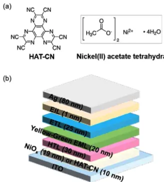
NiO
x가 HIL로 적용 가능한지를 확인하기 위해 OLED 소자 를 제작하고 분석을 진행하였다. Fig. 1(a)는 HAT-CN 과 NiO
x의 전구체인 nickel(II) acetate hydrate 분자구조이다. Fig. 1(b) 는 OLED 소자의 구조를 그림으로 나타낸 것이다. Fig. 2(b)는 사용된 재료의 에너지 밴드 다이어그램으로 각 재료들의 LUMO 및 HOMO 에너지 준위를 보여준다 [17]. 연구에 사용된 HTL, EML, ETL 은 개발중인 방향족 유기 단분자 재료로써 화학적 구 조와 같은 자세한 사항들은 공개할 수 없지만, 본 연구의 목적 인 HIL로써의 NiO
x특성을 검증하고 HAT-CN과 비교하는데 있 어서는 문제가 되지 않을 것으로 판단된다.
3.1 NiOx film의 전기적 특성 분석을 위한 OLED소 자 제작
Fig. 1. (a) Molecular structure of HAT-CN and NiO
xprecursor and
(b) the schematic of the OLEDs.
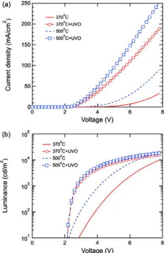
일반적으로 용액공정 기반의 sol-gel 방법으로 결정성이 우수 한 NiO
x박막을 형성하기 위해서는 300
oC의 고온이 필요한 것 으로 알려져 있다 [18]. 따라서 우리는 370, 500
oC의 두가지 온 도에서 열처리 공정을 진행한 NiO
x박막을 HIL으로 사용하여 OLED 소자를 제작, 분석하였다. 또한, 추가적으로 UVO 처리에 의한 전기적 특성 변화도 비교 분석하였다. Fig. 3(a),(b)는 각각 조건 별로 제작된 소자의 전류밀도(current density)-전압(voltage)- 휘도(uminance)-전압(voltage)의 분석 결과이다. 그래프에서 확 인할 수 있듯이 370
oC 보다 500
oC 의 열처리 온도에서 제작된 NiO
x박막을 OLED에 적용했을 때 전류밀도와 휘도가 향상되 었음을 알 수 있다. 이는 NiO
x를 고온인 500
oC 에서 열처리하 였을 때 우수한 전기 전도특성을 가지는 것을 알 수 있다. 추가 로, UVO 처리를 했을 때, 전류밀도와 휘도가 상승한 결과를 보 였다. 이러한 결과는 NiO
x박막에 UVO 처리를 진행했을 때, 일 함수가 증가하고 이로인해 HTL로의 정공주입 장벽이 감소하였 기 때문으로 해석된다 [17]. 이러한 분석을 통해 우리는 공정온 도 500
oC에서 형성된 NiO
x박막에 UVO 공정을 적용하는 조 건이 최적의 조건임을 확인하였다.
3.2 NiOx와 HAT-CN 의 정공 주입 특성 비교
앞서 최적화한 공정 온도 500
oC, UVO 처리를 한 조건의 NiO
x박막을 유기 HIL인 HAT-CN을 사용한OLED 소자와 비교 분석 하였다. 일반적으로 ITO는 고온에서 열처리 할 때 저항이 증가 하는 현상이 발생한다 [19]. 따라서 정확한 비교를 위해서 HAT- CN을 HIL로 사용한 OLED소자의 경우, 제작 전 ITO/Glass기 판을 동일하게 500
oC에서 40분 동안 열처리를 한 후에 공정을 진행하였다. HIL을 제외하고는 모두 동일한 재료로 OLED 소 자를 제작하여 소자 특성을 분석하였다. Fig. 4(a), (b), (c) 및 (d) 는 NiO
x와 HAT-CN을 각각 HIL로 사용한 OLED 소자의 전
류밀도-전압-휘도 특성 및 효율 특성을 보여준다. 전류밀도의 경 우 NiO
x는 6 V에서 147.76 mA/cm
2의 특성을 보였으며, HAT-CN 의 경우 6 V에서 91.94 mA/cm
2을 기록하였다. 이를 통해 NiO
x가 유기 반도체 재료인 HAT-CN보다 향상된 전기적특성을 보 여주는 것을 확인할 수 있다. NiO
x와 HAT-CN을 HIL로 적용했 을 때의 휘도는 각각 6 V에서 12,600 cd/m
2, 11,005 cd/m
2으로 NiO
x가 소폭 향상된 특성을 보인다. 그러나 최대 휘도는 NiO
x의 경우 18,505 cd/m
2, HAT-CN 의 경우 21,182 cd/m
2로 역전된 결과를 기록하였다. 이는 NiO
x의 정공주입능력이 HAT-CN보다 뛰어나 고전류 구동을 할 수록 전자와 정공의 비율(charge balance) 의 불균형이 심해져 exciton의 비발광성 재결합이 증가한 것으 로 예상된다. 이러한 특성은 Fig. 4(c)의 발광효율특성에서도 고 전류 구동에서의 효율저하가 NiO
x에서 더 급격하게 나타나는 것으로 확인된다.
발광효율 최대값의 경우에는 NiO
x의 경우 21.9 cd/A, HAT- CN의 경우 22.38 cd/A로 비슷한 수준을 기록하였다. 외부양자 효율은 NiO
x의 경우 6.72%, HAT-CN의 경우 6.85%의 최대값 을 가졌다. 전력효율의 경우에도 NiO
x의 경우 31.30 lm/W, HAT- Fig. 2. Flat-band energy band diagram of the OLEDs.
Fig. 3. (a) Current density-voltage characteristics and (b) luminance-
voltage curves of the OLEDs with various post-treated NiO
xthin films as HIL.
CN 의 경우 31.97 lm/W의 최대값을 기록하였으며, 발광효율과 마찬가지로 비슷한 수준임을 확인할 수 있었다. 결과적으로 향 상된 전류 특성으로 인해 1,000 cd/m
2의 동일 휘도의 구동 시 소비전력은 HAC-CN의 경우 0.74 mW였고, NiO
x의 경우 이보
다 낮은 0.54 mW로 소비전력이 37% 감소하였다.
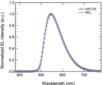
Fig. 5 의 경우에는 각각의 HIL에 따른 전계 발광(electroluminescent, EL) 스펙트럼이다. 스펙트럼의 최대값은 544 nm으로 동일한 위치 를 기록하였다. 즉, 유기 반도체 재료인 HAT-CN 대신 NiO
x를 사 용하여도 발광 특성은 변하지 않는 것으로 판단된다.
OLED 소자 특성 분석 결과 NiO
x는 HIL으로서 유기 반도체 재료인 HAT-CN 보다 전기적인 특성이 향상되었으며, 휘도, 발 광 효율의 경우에는 비슷한 수준을 기록하였다. 이는 전이금속 산화물계 재료인 NiO
x가 정공주입층으로서 유기재료를 대체하 여 적용 가능함을 알 수 있다. 이러한 NiO
x박막은 OLED 뿐만 아니라 유기센서, 유기태양전지 등 다양한 유기전자소자에도 사 용 가능 할 것으로 생각된다. 그러나, 박막 형성을 위한 공정 온 도가 높기 때문에 저온 공정 개발이 필요할 것이며, 하부 층을 고려하여 소자의 설계가 되어야 할 것이다.
4. 결 론
본 연구에서는 수분과 산소에 취약한 유기 반도체 재료를 무 기 재료인 전이금속산화물 NiO
x로 대체하고자 OLED 소자를 Fig. 4. (a) Current density–voltage, (b) luminance–voltage, (c) current efficiency, and (d) power efficiency characteristics of the OLEDs using
HAT-CN or NiO
xas HIL.
Fig. 5. Normalized electroluminescent spectra of OLEDs based on
HAT-CN or NiO
xas HIL.
제작 및 분석을 진행하였다. NiO
x박막의 특성을 향상시키고자 공정 온도 최적화 및 UVO처리를 진행하였고, OLED 소자를 제 작하여 유기 반도체 기반의 HIL인 HAT-CN과 동등한 수준의 특성을 확인하였다. 또한, 이러한 결과를 통해 NiO
x가 유기 반 도체 재료를 대체할 수 있는 무기물 기반의 전이금속산화물 재 료라는 결과를 얻을 수 있었다.
무기 재료 기반의 HIL인 NiO
x박막은 OLED 뿐만 아니라 다 양한 유기전자소자에 적용이 가능할 것으로 기대된다. 또한 무 기 재료인 NiO
x의 경우에는, 산소와 수분에 취약한 유기재료의 단점을 보완할 수 있기 때문에 수명의 향상이 기대된다.
감사의 글
이 연구는 금오공과대학교 학술연구비로 지원되었다 (2019104037).
REFERENCES