Polarizer-free, high-contrast inverted
top-emitting organic light emitting diodes:
effect of the electrode structure
Hyunsu Cho and Seunghyup Yoo*Department of Electrical Engineering, Korea Advanced Institute of Science and Technology (KAIST), 373-1 Guseong-dong, Daejeon 305-701, South Korea
Abstract: Circular polarizer (CP)-free, high-contrast inverted top-emitting organic light-emitting diodes (ITOLEDs) are demonstrated by using a semitransparent Ag electrode capped with a single dielectric layer as a top anode and Cs2CO3 (1.5 nm)/Al (1.5 nm)/Cr (100nm) as a partially absorbing bottom cathode. Low luminous reflectance is achieved by combining the broadband absorption of Cr, the weak but inherent cavity structure, and the optimal thickness of the capping layer yielding a high transmittance of a top electrode. With the optimized organic capping layer, contrast-enhanced ITOLEDs exhibit a luminous reflectance as low as 3.6% with a large thickness margin. Their luminous efficiency is shown to be comparable to or even higher than that of CP-based conventional OLEDs. ©2012 Optical Society of America
OCIS codes: (230.3670) Light-emitting diodes; (230.4170) Multilayers; (310.6845) Thin film
devices and applications; (310.6860) Thin films, optical properties.
References and links
1. S. Reineke, F. Lindner, G. Schwartz, N. Seidler, K. Walzer, B. Lüssem, and K. Leo, “White organic light-emitting diodes with fluorescent tube efficiency,” Nature 459(7244), 234–238 (2009).
2. A. N. Krasnov, “High-contrast organic light-emitting diodes on flexible substrates,” Appl. Phys. Lett. 80(20), 3853–3855 (2002).
3. H. Aziz, Y.-F. Liew, H. M. Grandin, and Z. D. Popovic, “Reduced reflectance cathode for organic light-emitting devices using metalorganic mixtures,” Appl. Phys. Lett. 83(1), 186–188 (2003).
4. W. Ji, L. Zhang, Z. Tianyu, W. Xie, and H. Zhang, “High-contrast and high-efficiency microcavity top-emitting white organic light-emitting devices,” Org. Electron. 11(2), 202–206 (2010).
5. C.-J. Yang, C.-C. Lin, C.-C. Wu, Y.-H. Yeh, C.-C. Cheng, Y.-H. Kuo, and T.-H. Chen, “High-contrast top-emitting organic light-top-emitting devices for active-matrix displays,” Appl. Phys. Lett. 87(14), 143507 (2005). 6. S. M. Chen, Y. B. Yuan, J. R. Lian, and X. Zhou, “High-efficiency and high-contrast phosphorescent
top-emitting organic light-top-emitting devices with p-type Si anodes,” Opt. Express 15(22), 14644–14649 (2007). 7. C. Py, D. Poitras, C.-C. Kuo, and H. Fukutani, “High-contrast organic light emitting diodes with a partially
absorbing anode,” Opt. Lett. 33(10), 1126–1128 (2008).
8. C.-C. Wu, C.-W. Chen, C.-L. Lin, and C.-J. Yang, “Advanced organic light-emitting devices for enhancing display performances,” J. Display Technol. 1(2), 248–266 (2005).
9. J. Huang, Z. Xu, and Y. Yang, “Low-work-function surface formed by solution-processed and thermally deposited nanoscale layers of cesium carbonate,” Adv. Funct. Mater. 17(12), 1966–1973 (2007).
10. H. Cho, C. Yun, J.-W. Park, and S. Yoo, “Highly flexible organic light-emitting diodes based on ZnS/ Ag/ WO3
multilayer transparent electrodes,” Org. Electron. 10(6), 1163–1169 (2009).
11. C. Yun, H. Cho, H. Kang, Y. Lee, Y. Park, and S. Yoo, “Electron injection via pentacene thin films for efficient inverted organic light-emitting diodes,” Appl. Phys. Lett. 95(5), 053301 (2009).
12. L. A. A. Pettersson, L. S. Roman, and O. Inganäs, “Modeling photocurrent action spectra of photovoltaic devices based on organic thin films,” J. Appl. Phys. 86(1), 487–496 (1999).
13. H. Cho, C. Yun, and S. Yoo, “Multilayer transparent electrode for organic light-emitting diodes: tuning its optical characteristics,” Opt. Express 18(4), 3404–3414 (2010).
14. D. G. Deppe, C. Lei, C. C. Lin, and D. L. Huffaker, “Spontaneous emission for planar microstructures,” J. Mod. Opt. 41(2), 325–344 (1994).
15. D. Poitras, C.-C. Kuo, and C. Py, “Design of high-contrast OLEDs with microcavity effect,” Opt. Express
16(11), 8003–8015 (2008).
16. H. Riel, S. Karg, T. Beierlein, B. Ruhstaller, and W. Rieß, “Phosphorescent top-emitting organic light-emitting devices with improved light outcoupling,” Appl. Phys. Lett. 82(3), 466–468 (2003).
17. C.-L. Lin, H. W. Lin, and C.-C. Wu, “Examining microcavity organic light-emitting devices having two metal mirrors,” Appl. Phys. Lett. 87(2), 021101 (2005).
18. M. Thomschke, S. Hofmann, S. Olthof, M. Anderson, H. Kleemann, M. Schober, B. Lüssem, and K. Leo, “Improvement of voltage and charge balance in inverted top-emitting organic electroluminescent diodes comprising doped transport layers by thermal annealing,” Appl. Phys. Lett. 98(8), 083304 (2011).
19. C.-W. Chen, C.-L. Lin, and C.-C. Wu, “An effective cathode structure for inverted top-emitting organic light emitting devices,” Appl. Phys. Lett. 85(13), 2469–2471 (2004).
20. C. Yun, H. Cho, T.-W. Koh, J.-H. Kim, J. W. Kim, Y. Park, and S. Yoo, “Doping-free inverted top-emitting organic light-emitting diodes with high power efficiency and near-ideal emission characteristics,” IEEE Trans. Electron. Dev. 59(1), 159–166 (2012).
1. Introduction
There has been a great deal of interest in organic light-emitting diodes (OLEDs) due to their various advantages in displays and lighting [1] When used for displays, OLEDs must be easily recognizable under ambient illumination. However, this objective is challenging for native OLED geometry due to the presence of reflective metal electrodes. Under conditions of bright illumination, the reflected light can be comparable to the light emitted from OLEDs and the resultant level of contrast can become poor. This problem can be circumvented by attaching a circular polarizer (CP), which consists of a quarter-wave plate and a linear polarizer, to the opposite side of a substrate. This method is very effective in suppressing the ambient light reflection but also incurs additional production costs. In addition, the relatively thick CP could impose a limitation on the making highly flexible nature of OLEDs. Hence there have been numerous studies devoted to the development of CP-free high contrast ratio (CR) OLEDs [2–7].
There are two major strategies proposed for CP-free high-CR OLEDs. The first type involves the use of highly absorbing layers, often called “black layers”, right in front of the reflecting electrodes [2–4]. The second type involves the use of a carefully designed multilayer thin-film structure which consists of an OLED and additional layer assemblies and functions as a whole like an anti-reflection (AR) coating [5–7]. The second approach has recently been attracting attention because it can potentially yield high-CR OLEDs with efficiency that exceeds those of CP-based OLEDs [5]. This is because the internally generated light that moves toward the back electrode is not completely lost in the second approach and/or efficiency enhancement due to a microcavity effect can be expected. The work of Py et al. exemplified the second approach: they proposed a high-CR OLED structure in which a multilayer filter consisting of a partially absorbing metal layer and a distributed Bragg reflector is stacked on a conventional microcavity-type OLED to strike a balance between the microcavity effect for emitted light and the low reflection for incident ambient light [7]. To the same end, Wu and his associates replaced a bottom metal electrode in top-emitting OLEDs with a partially reflecting and absorbing electrode; they demonstrated a luminous efficiency larger than that of ITO/CP-based high CR OLED along with low reflectance throughout the visible spectrum [5]. Our work proposes a high-CR structure for an inverted top-emitting OLED (ITOLED) configuration; this type of configuration is important because of its benefits when used with emerging backplane technologies that are based on n-type amorphous oxide thin-film transistors [8]. Considering that the success of these AR-coating approaches relies not only on its effectiveness but also on the simplicity in structure and fabrication in practice, we propose a simple top-emitting geometry with a semitransparent electrode capped with a single dielectric layer used together with a partially absorbing bottom electrode. A particular attention is paid to a proper choice of the capping layer with a suitable thickness and to a right combination of the bottom cathode assembly yielding an efficient electron injection so that an optimal structure ensuring a low reflectance and high brightness can be established.
2. Experiment
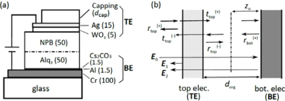
Figure 1(a) shows the structure of the proposed CP-free high-CR ITOLED. It has a 100-nm-thick layer of Cr as a partially absorbing bottom electrode (cathode) and a 15-nm-100-nm-thick layer
Fig. 1. (a) The device structure of the proposed circular polarizer (CP)-free high contrast ratio (CR) ITOLED. The number in parenthesis indicates the thickness of the corresponding layer given in nm. (b) The schematic diagram for the simplified multilayer geometry used for thin-film optic calculation. The letters stand for the Fresnel coefficients and electric fields relevant to the calculation done in this work.
of Ag as a semitransparent top electrode (anode). For efficient carrier injection from the Cr electrode, we inserted very thin layers of Al (1.5nm) and Cs2CO3 (1.5nm) between the Cr layer and a layer of tris(8-hydroxy-quinolinato) aluminum (Alq3) (50nm), which is used as an emission/ electron transporting layer (EML/ ETL) [9]. Likewise, a layer of WO3 (5nm) is inserted for efficient hole injection between Ag and a hole transport layer of N,N'-bis(naphthalen-1-yl)-N,N'-bis(phenyl)-benzidine (NPB) (50nm). A layer of ZnS (35nm) or Alq3 (60nm) is deposited on top of the Ag electrode as a capping layer. A combination of a WO3 layer, Ag, and a dielectric capping layer may be viewed as an alternative type of a dielectric-metal-dielectric multilayer transparent electrode; it works as an effective anode for the bottom electrode geometry [10] and the top electrode geometry [11]. Cr is deposited by sputtering on a pre-cleaned glass substrate; all other depositions are made by thermal evaporation in a vacuum chamber (HS-1100, Digital Optics & Vacuum). A source-measure unit (Keithley 2400) and a calibrated photodiode were used to measure the current density-voltage-luminance (J-V-L) characteristics in a N2-filled glove box. A UV-VIS spectrometer (SV2100, K-MAC) was used to measure the reflectance in air.
Optical analysis was based on transfer matrix formalism (for the reflectance, transmittance, and phase) [12] and on a microcavity model (for the light output from OLEDs) [13,14]. The optical constants used for the calculation were borrowed from the literature or measured by means of spectroscopic ellipsometry [13]. As the figure of merit for the CR performance, we used luminous reflectance, RL(λ), which is defined as follows [15]:
( ) ( ) ( ) ( ) ( ) OLED L V S R d R V S d λ λ λ λ λ λ λ =
∫
∫
(1)where S(λ) is the spectrum of a standard ambient light source (We used the CIE standard light source D65), V(λ) is the photopic response of the human eye sensitivity, and ROLED(λ) is the reflectance spectrum of an OLED under test [15].
3. Results and discussions
3.1 The optimal optical structure of the proposed high-CR OLEDs
Figures 2(a) and 2(b) present the measured optical constants (n, k) and reflectance spectra
Rbot(λ) of the Cr layer under study. The simulated curve (solid line in Fig. 2(b)) for Rbot(λ), obtained with those optical constants, show quantitative agreement with the experimental data. As desired, Rbot(λ) is confirmed to be relatively low throughout the visible spectrum. At λ of 520nm, for example, R(λ) is 34.5% when the light is incident from air to the Cr layer. This value is translated into Rbot(λ) of approximately 18.9% when the light is incident from the organic layer (n = 1.74) to the Cr layer (as indicated by the dashed line in Fig. 2(b)).
Fig. 2. (a) Optical constants (n, k) of the Cr and (b) calculated and measured reflectance spectra of the Cr layer for light incident from air (solid line) or from organic layer (dashed line).
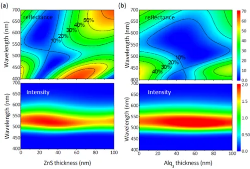
With the Cr layer used as a bottom electrode in the proposed top-emitting OLED geometry, we calculated the reflectance, ROLED (in %), and the light emission, IOLED (in arbitrary units), from the total OLED structure as a function of the capping layer thickness (dcap) and λ for the capping layers of ZnS and Alq3. (See each column in Figs. 3(a) and 3(b)) Note that for both types of capping layers, there is an optimum dcap which can result in a relatively low ROLED in most of the visible spectral region. In such an optimum case, RL for devices with ZnS and Alq3 turns out to be as small as 3.9% and 2.3%, respectively.
Fig. 3. Calculated reflectance ROLED (in %) and the light emission IOLED (in arbitrary units) from
the total OLED structure as a function of the capping layer thickness (dcap) and wavelength (λ)
for capping layers of (a) ZnS and (b) Alq3.
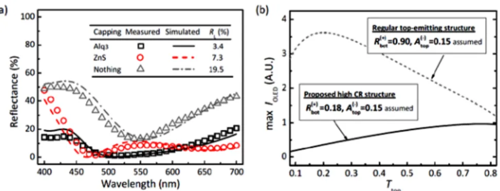
Figure 4(a) shows the experimental reflectance spectra obtained for dcap of 35nm (ZnS) and 60nm (Alq3), both of which are close to their respective optimum dcap. RL in these devices turned out to be 7.3% (ZnS) and 3.4% (Alq3). These relatively low values, which are comparable to or lower than those of typical CP-based OLEDs (~4%) [5], confirm that the effectiveness of the proposed simple, single-capping-layer geometry in obtaining a high-CR without a CP.
Fig. 4. (a) Experimental and simulated reflectance spectra from the total OLED structure with capping layers of: Alq3, ZnS, and nothing. (b) Trend of maximum IOLED vs. Ttop for the
proposed ITOLEDs and regular top-emitting OLEDs. Δφ rt is set as 2mπ (m: integer) in (b).
In addition to its effectiveness for low RL, Fig. 3 further reveals that (i) the optimum condition for RL almost coincides with that for the maximum light output for both types of OLEDs; and that (ii) the ranges of dcap and λ that correspond to the low ROLED are much wider for devices with an Alq3 capping layer than for devices with a ZnS capping layer. The same behavior occurs also for the range of dcap that corresponds to a high IOLED near the emission wavelength (~520 nm). In fact, IOLED varies only slightly (that is, less than 20% from the peak) when dcap varies from 0nm to 100nm in case of the Alq3 capping. Note that such insensitiveness is rarely observed in conventional top-emitting microcavity-based OLEDs; the
IOLED of the latter strongly depends on dcap [16].
To better understand the mechanism behind these trends, we applied a simplified approach to the proposed ITOLED structure. In particular, we considered the fact that the intensity of the light attenuates significantly when the light is reflected from the bottom electrode of the proposed ITOLED structure. (Recall that Rbot is 0.17 to 0.20 throughout the visible spectral region.) In such a case, only the wave components that experience one or two reflections are effectively meaningful. Consequently, cavity-enhancement effect is relatively low, which means that neither ROLED nor IOLED is influenced much by the infinite number of multiple reflections, even when the cavity resonance conditions are met. As a result, the electric fields for the reflected light (Erefl) and emitted light (EOLED), which are related to the electric fields of the incident light (E0) and internally generated light (EEML), respectively, can be expressed as follows: org 0 org 4 ( ) ( ) ( ) ( ) 1 2 0 4 4 ( ) ( ) ( ) ( ) 1 1 i nd
refl top top top bot
i nz i nd
OLED top EML bot top bot
E E E E r t t r e E t E r e r r e π λ π π λ λ + + − + − + − + ≈ + = + ≈ + + (2)
where E1 is the field reflected right from the top electrode and E2 is the field that returns after the first reflection from the bottom electrode. ttop(bot) and rtop(bot) refer to the local Fresnel transmission and reflection coefficients for the top (bottom) electrode assembly, respectively, and they are generally complex numbers. ‘+’ (‘–’) signs in the superscript indicate that the corresponding variable is defined for the light that moving from left to right (right to left) in Fig. 1 (b). Using Eq. (1), we can express the equations for ROLED and IOLED as follows:
(
)
( ) 2 ( ) ( ) ( ) ( )
1 / 2 / cos
OLED top top bot top top bot top refl OLED EML FP TB R R T R R T R R I I f f ϕ + + + + + ≈ + + ∆ ≈ (3) where
(
)
(
)
( ) ( ) ( ) ( ) 2 1 ( ) ( ) ( ) ( ) 2 1 1 2 cos , 4 tan /FP top top bot top bot rt
refl org org ttop ttop rbot rtop
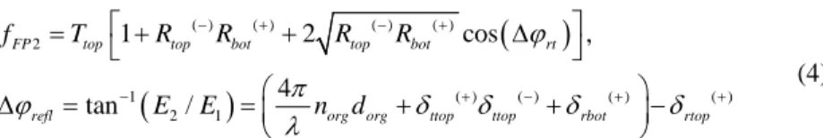
f T R R R R E E n d ϕ π ϕ δ δ δ δ λ − + − + − + − + + = + + ∆ ∆ = = + + − (4)
and Ttop is the local transmittance of the top electrode, fFP2 is a two-beam version (rather than the typical infinite-beam version [13]) of the Fabry-Perot term, and fTB is the two-beam interference factor. Expression for fTB in the proposed devices is not different from that of the conventional devices [13]. δrbot( + ) and δrtop(-) are the phases of rbot( + ) and rtop(-), respectively.
Several observations can be made from the above Eqs. (3) and (4). Firstly, ROLED is reduced to zero by the destructive interference when Rtop(+) = Rbot(+)Ttop2 (that is, the intensity balance between E1 and E2) and Δφ refl = (2m + 1)π where m is the integer number (that is, phase reversal between E1 and E2). Secondly, fFP2 and IOLED are monotonically increasing functions of Ttop and reach their maximum level when the round-trip phase difference Δφ rt = 2mπ (phase matching) in most cases as shown in Fig. 4(b). This is because the present OLED structure has a very limited cavity resonance effect. Note that this trend is in contrast with the case of typical top-emitting OLEDs, IOLED of which peaks at a relatively small Ttop (a large
Rtop) as can be seen from the gray, short-dashed curve in Fig. 4(b) [17].
For optimization, one should look for the conditions that simultaneously lead to a low
ROLED and high IOLED. It has to be kept in mind that the conditions for a low ROLED should be
fulfilled as much as possible throughout the visible spectrum whereas the conditions for high
IOLED could be fulfilled only around the emission wavelength. Figure 5 presents each parameter of the devices under study near the optimum condition shown in Fig. 3. One can see that the optimized device structure indeed fulfills the design guidelines outlined above. Let us take an example of ITOLEDs with a 60-nm-thick Alq3 capping layer. First, it can be seen that Δφrt (≈-0.05π) is close to zero near λEML so that light emission from these ITOLEDs is enhanced. Under this condition, Δφrefl (≈0.96π) becomes close to π due to the inherent complementary phase relation between the Δφrefl and Δφrt of the metal-dielectric-metal microcavities [15], automatically fulfilling the low ROLED at least near λEML. As for balancing of the intensity between the major reflected components, the optimal transmittance of the top electrode may be found by solving Rbot(+)Ttop2 = Rtop(+) = 1- Atop(+)-Ttop for Ttop. With Rbot(+) of (20 ± 5)% and At
(+)
of 15%, the optimal Ttopis estimated to be (74 μ 2)%. This value is quite close to what occurs near λEML (Table 1). In fact, such a high transmittance is close to the maximum Ttop that can be accessed in the given top electrode structure upon variation of dcap. This behavior, together with the aforementioned phase relation and the fact that IOLED increases with Ttop, explains why ROLED and IOLED share a common optimum for dcap in the proposed ITOLED devices.
In the spectral region that is relatively far from λEML, a low ROLED can be attained by means of several different mechanisms. Since the strict phase condition for a low ROLED is not
Fig. 5. Calculated ROLED, Rtop, Ttop2Rbot(+), and Δφrefl to monitor the intensity and phase
relationships between the reflected components E1 and E2 in devices under study for the cases
of (a) no capping, (b) ZnS-capping, and (c) Alq3-capping. Inset: Calculated absorption within
Table 1. Optical components of the simplified device diagram with different capping layers*
Capping layer Ttop (%) Rtop(+) (%) Rbot(+)Ttop2 (%) Rbot(+)Ttop2/Rtop(+)
Nothing 52.4 38.0 5.1 0.13 ZnS 77.8 7.2 11.4 1.58 Alq3 73.1 11.4 10.0 0.88
* R
bot(+) is common as 18% for all the cases. All calculation was done at λ = λ EML = 520 nm
fulfilled in this spectral region, the intensity of the major reflected light components can become a more important factor. For example, a low ROLED may be attained by having a low
Rtop( + ); in this case, the overall intensity of E1, which is generally the most significant reflected component, can be kept low regardless of the interference effect. Likewise, a low
ROLED may be attained if the intensity is balanced at more than one wavelength. ZnS- or Alq3 -capped devices not only have a low Rtop(+) in general but also have multiple wavelengths where intensity values of E1 and E2 are balanced. In the ZnS-capped devices, the intensity balance is achieved at two different wavelengths to result in ‘W-shaped’ ROLED spectrum shown in Fig. 5(b). In the Alq3-capped devices, the intensity balance is fulfilled over the spectral “band” of 510 nm to 580 nm also to result in low ROLED throughout the visible spectrum. On the other hand, the device without a capping layer suffers from a relatively high
Rtop(+) and, consequently, a relatively large ROLED. The high level of Rtop(+) ( = low Ttop) in the device without a capping layer makes it hard to find a wavelength that can fulfill the intensity balance condition, further aggravating the situation. (See Fig. 5(a)).
The fact that the Alq3-capped devices meet the intensity balance conditions over the relatively broad spectral band results partly from the low spectral variation of Rtop(+). Note that this is consistent with the insensitiveness of their ROLED and IOLED to λ and dcap. This is because the optical properties are determined not by the physical thickness but by the optical thickness. Since the refractive index of Alq3 (1.7 ~1.8) is smaller than that of ZnS (2.3 ~2.5), the change in the optical thickness of the Alq3 layer is smaller than that of the ZnS layer for the same change in physical thickness. Such insensitiveness is expected to be highly beneficial in a real manufacturing because a certain target RL can be easily met with a wide margin for dcap.
Another feature that Alq3 capping layers can offer is the selective absorption in the blue-UV region (Inset in Fig. 5(b)). The 60-nm-thick Alq3 capping layer absorbs approximately 40% of the photons with λ of 400 nm. This effectively suppresses Rtop(+) and ROLED in the UV-blue spectral range, further helping the OLEDs with an Alq3 capping layer produce RL as low as 3.6% with the improved spectral neutrality. It should be noted that such absorption can be disadvantageous in case of blue OLEDs. Nevertheless, it should not be too much of concern because there are numerous materials that are transparent in the blue spectral region and have refractive indices similar to that of Alq3.
3.2 Device performance of the ITOLEDs: electron injection from the proposed bottom electrode
Electron injection from a bottom cathode is a major limiting factor in inverted OLEDs. Thus, finding a suitable combination of an electrode and injection layer has been the key step in developing sustainable inverted OLEDs. Thomschke et al., for example, inserted a layer of 4,7-diphenyl-1,10-phenanthroline (Bphen) doped with Cs and Ag in between the Ag bottom electrode and a Cs-doped Bphen layer to reduce the operating voltage and improve the carrier balance in an inverted top-emitting geometry [18]. Similarly, Chen, Lin, and Wu inserted an ultrathin trilayer of Alq3/LiF/Al in between the Ag bottom electrode and an Alq3 layer [19]. Recently, it was found that a thermally evaporated ultrathin layer of Cs2CO3, which works as an electron injection layer (EIL) when used with an Al top electrode, can work as an EIL with a bottom cathode as well [20]. However, the bottom cathode in that study was also with an Al layer, so it may not be directly applicable to the present case, which requires a partially absorbing electrode such as Cr (this work) or Mo [5].
Fig. 6. J-V characteristics of electron-only devices in the configuration of glass/ Cr (200nm)/ x / Alq3 (100nm)/ Ca (50nm)/ Al (100nm) where x is Cs2CO3 (1.5nm), Al (1.5nm)/ Cs2CO3
(1.5nm), or nothing.
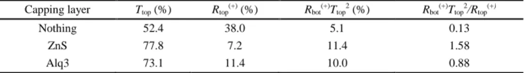
Figure 6 shows the current density (J) - voltage (V) characteristics of electron-only devices with the following configuration of glass/ Cr (200nm)/ x / Alq3 (100nm)/ Ca (50nm)/ Al (100nm) where x is Cs2CO3 (1.5nm), Al (1.5nm)/ Cs2CO3 (1.5nm), or nothing. The top Al electrode is biased positively so that electrons are injected from the bottom electrode (Cr). The results confirm that the deposition of the ultrathin Cs2CO3 layer alone cannot improve the electron injection. Instead, it shows that insertion of an additional ultrathin Al layer between the Cr and Cs2CO3 layers is essential in achieving enhancement of the electron injection. This observation appears to be consistent with the previous reports suggesting the beneficial role of Al in making Cs2CO3 layers effective EILs in top cathode configurations [9] and bottom cathode configurations [20].
Fig. 7. (a) J-V-L and (b) L-J characteristics of the proposed ITOLEDs with the capping layer of nothing, ZnS, or Alq3. Inset in (b): The photograph of the Alq3-capped ITOLED under
operation.
Figure 7 shows the current density-voltage-luminance (J-V-L) and J-L characteristics of the OLEDs under study. The photograph of the Alq3-capped device is also shown in its inset. With the bottom cathode configuration of Cr (100nm)/ Al (1.5nm)/ Cs2CO3 (1.5nm), the proposed ITOLED devices exhibit a turn-on voltage (=the onset voltage for luminance of 1 cd/m2) as low as 3.5V, which is comparable to the typical turn-on voltage of conventional NPB/ Alq3-based OLEDs (≈2.5V) [10]. Moreover, the device with the 60-nm-thick Alq3 capping layer exhibits a current efficacy of about 2.2 cd/A, which is twice as high as that of devices without capping layer and comparable to or slightly higher than that of conventional bottom-emitting OLEDs based on NPB/Alq3 with a CP [5]. Although it is unlikely to obtain a large enhancement of luminous efficiency in the proposed ITOLED devices due to the low
Rbot( + ), which tends to induce a relatively low cavity enhancement effect, a part of the light emitted toward the bottom electrode still survives the reflection at the Cr electrode. This surviving light consequently contributes to the overall external light emission to some degree
and leaves room for improvement in luminous efficiency. Such improvement may be realized if one can increase Rbot while maintaining RL low.
4. Conclusions
In summary, we investigated circular-polarizer (CP)-free high-CR inverted emitting top-emitting OLEDs (ITOLEDs). To produce them with a relatively simple structure, we examined whether a top-emitting geometry with a single dielectric capping layer would be sufficient for this purpose. Our results confirm that a properly chosen capping layer and a partially absorbing bottom electrode structure are an effective solution for CP-free high-CR OLEDs. A capping layer of Alq3, the refractive index of which is high but not too high, provides low reflectance throughout the visible spectral range with a relatively low dependence on its thickness and the wavelength of the light. Together with the absorption in the UV-blue spectral region, the proposed ITOLEDs with the optimized Alq3 capping layer exhibit a low luminous reflectance of 3.6% with improved spectral neutrality. The proposed bottom electrode, which consists of a Cr layer covered with thin Al/ Cs2CO3 layers, effectively injects electrons to Alq3 layers and consequently produces a low turn-on voltage. Despite the relatively low microcavity effect, the optimized devices have a luminous efficacy that is comparable to or slightly higher than that of conventional bottom-emitting OLEDs with CP. Given the simplicity of the structure and the benefits of ITOLEDs, the study shown here provides important information for producing cost-effective high-CR OLEDs that are compatible with emerging backplane technologies.
Acknowledgment
This work was supported by the RFID R&D program of MKE/KEIT (10035225, Development of core technology for high performance AMOLED on plastic).