Photonic Bandgap Structures with Arrays of Spiral metal Patches
Wonjune Jho
*, Donghyuk Yeom
*, Changjoon Yoon
*Kyoungah Cho
+, and Sangsig Kim
*★Abstract
A new type of photonic bandgap(PBG) structures that consist of arrays of spiral metal patches is proposed in this paper. Reflection phases and radiation of these PBG structures are simulated by high frequency structure simulator(HFSS) to characterize their performance. The simulation results show that the resonant frequency of the proposed PBG structures gets significantly lower than those of the PBG structures with square metal patches, but that the radiation is nearly the same for both of the PBG structures. Analysis on reflection phases reveals that the lowering of the resonant frequency is associated with the increase in capacitance.
Key words: PBG, HFSS, reflection phase, radiation, resonant frequency
* Department of Electrical Engineering, Korea University
+ Institute for Nano Science, Korea University
★Corresponding author : [email protected]
I. Introduction
Incorporation of a special texture on a metal plate can alter the electromagnetic properties of this metal plate in the radio frequency range. The texture consists of a two-dimensional array of metal protrusion on the metal plate. In the textured metal plate, phase of reflected electromagnetic wave does not change on its surface. Moreover, the textured metal plate can have much higher surface impedance than a smooth one, thereby suppressing surface current [1]. Because of these electromagnetic properties, the textured metal plate has been used for the fabrication of TEM wave-guides [2,3], antennas [4], filters [5], and amplifiers [6].
The interference of electromagnetic wave caused by the incorporation of a periodic texture on a metal plate prevents them from propagating at a finite frequency band, giving rise to a
two-dimensional electromagnetic bandgap [7]. The
textured metal plate can be accordingly considered as a two-dimensional photonic crystal, and the periodic texture is called a photonic-bandgap(PBG) structure which has been widely researched so far [8-10]. PBG structures consisting of an array of square metal patches connected to the ground plate by thin metal vias have been widely investigated [11]. This two-dimensional PBG structure illustrated in Fig. 1 has been analyzed as a parallel LC resonant circuit. A unit cell of this PBG structure is comprised by inductance L and capacitance C;
inductance is associated with the via between the patch and ground plate, and capacitance is a capacitance between the patches.
Phase of electromagnetic wave reflected on a smooth metal plate changes by 180°, but the phase shift (or, the reflection phase) of electromagnetic wave on the surface of the PBG structure slopes down from 180° to -180° with raising frequency, as illustrated in Fig. 2. For the PBG structure, the reflection phase crosses through 0° at the resonant frequency (Wo) ; Wo=(LC)-1/2. The bandwidth(△
W/Wo) of the reflection phase over the range from 90° to -90° is proportional to (L/C)1/2 [8]. As the capacitance increases, or as the resonance frequency reduces, the bandwidth narrows.
Fig. 1. An unit cell of the PBG Structure with square patches. The width of the metal patchs (w), the gap between the metal patchs (g), the height of the vias (t), the distance between the vias (l), and the length (a), capacitance (C), and inductance (L) of the unit cell are denoted in this schematic.
Capacitance and inductance of the PBG structure should increase for its use in the low frequency ranges of wireless communication circuits [1]. For the achievement of its increased capacitance and inductance, the PBG structure should enlarge physically. But, the enlargement of the PBG structure is not consistent with the requirement for the fabrication of the compact RF devices. The lowering of resonant frequency has therefore been investigated without the enlargement. A PBG structure developed recently by D. Sievenpiper’s group has attracted wide attention, since this structure achieves a lower operating frequency for a given thickness by using capacitive loading while reducing its physical size [1]. In this PBG structure, parallel-plate capacitors are formed by the top two overlapping layers. Nevertheless, this PBG structure has a serious disadvantage of complicated fabrication. Two masks are needed for the fabrication of the layers 1 and 2 of the top plates and the number of etching steps increases.
A new type of PBG structures that consist of arrays of spiral metal patches is proposed in this study to increase their capacitance and inductance for the achievement of lower resonant frequency than the PBG structure with square metal patches while still maintaining their simple fabrication procedure. In this paper, reflection phase and radiation of the proposed PBG structures are characterized by the High Frequency Structure
Simulator(HFSS), and then they are compared with the PBG structures with square metal patches.
Fig. 2. Representative reflection phase of electromagnetic wave reflected on the PBG structure.
2. Simulated Refection Phase of PBG Structures with Spiral Metal Patches
The PBG structures with spiral and square metal patches are depicted in Fig. 3; they are henceforth referred to as spiral and square PBG structures, respectively. The spiral PBG structure (Figs. 3(a) and 3(b)) proposed in this study has the same geometry as the square PBG structure (Fig. 3(c)) except the structure of the metallic patches. In the patches of the spiral PBG structure, four metal lines are turned once spirally and the central part is still square (Fig. 3(b)). For these two PBG structures, the lattice constant is 200 mils and the diameter of the cylindrical via is 10 mils. The volume below the square patches are filled with a material with a dielectric constant of 4.3, and the total thickness is 60 mils. For the square PBG structure, the spacing between the patches is 5 mils, but the spiral PBG structure does not have any spacing between the patches.
For the spiral and square PBG structures, reflection phase as a function of frequency was simulated by HFSS. In this simulation, three following assumptions were made; standing wave is perpendicular to the propagating direction, the upper and lower sides of wave-guide (parallel to the
propagating direction) are made of perfect conductor wall, and the left and right sides of wave-guide (perpendicular to propagating direction) are made of perfect magnetic wall. The reason for the third is that there must be no interference to propagating
standing waves.
Fig. 3. PBG structures with spiral(a and b) and square (c) metal patches. Detailed geometry for the spiral PBG structure is given in Fig. (b).
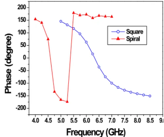
Simulated reflection phases for the spiral and square PBG structures are plotted in Fig. 4. The resonant frequency determined from the curve of reflection phase is 4.64 and 6.32 GHz, for the spiral and square PBG structures, respectively. The resonant frequency gets significantly lower for the spiral PBG structure, compared with the square
PBG structure. The lowering of the resonant frequency is caused by the increase in capacitance rather than inductance. Since the total thickness is the same for both of the PBG structures, the inductance is not likely to change. The plot illustrates also that the bandwidth narrows from 1.5 to 0.5 GHz. The narrowing of the bandwidth is associated with the lowering of the resonant frequency and the increase in capacitance. The narrowing is more attribute to the increase in capacitance than the lowering of the resonant frequency.
4.0 4.5 5.0 5.5 6.0 6.5 7.0 7.5 8.0 8.5 9.0 -200
-150 -100 -50 0 50 100 150 200
P h a s e ( d e g re e )
Frequency (GHz)
Square Spiral
Fig. 4. Reflection phases for the spiral and square PBG structures.
The structure of the metal patch in the spiral PBG structure includes four metal lines turned once spirally (see Fig. 3(b)). Each of the four metal lines begins to turn at each of four corners in the central square. The reason for this structuring is to minimize the variation of the capacitance as a function of direction in two-dimensional space. A spiral PBG structure different from the proposed PBG one in this study was simulated to examine how the variation affects characteristics of reflection phase. The metal patch in this different spiral PBG structure includes a metal line turned spirally. Its detailed geometry is depicted in Fig.
5(a). Fig. 5(b) shows that the simulated curve of reflection phase has spikes. These spikes are not seen in the curve of reflection phase for the proposed spiral PBG structure. These spikes are
due to the variation of the capacitance as a
function of direction.
Fig. 5. A spiral PBG structure with metal patches containing a metal line turned spirally; its detailed geometry (a) and reflection phase (b).
Spiral PBG structures with four different lengths of the metal lines on their patches were simulated to attain the better understanding of characteristics of reflection phase for the spiral PBG structures under study. Three different spiral PBG structures are given in Fig. 6; fourth one is the PBG structure shown in Fig. 3(b). The size of each metal plate in these PBG structures is the same as that of the square PBG structures, and the width of the metal lines and the distance between the metal lines are also the same for all the four spiral PBG structures. Simulated reflection phases are plotted as a function of frequency for the four different spiral PBG structures in Fig. 7. The plot shows that, as the length of the metal line is longer, the resonant frequency gets lower and the bandwidth
gets narrower. This lowering of the resonant frequency and the narrowing of the bandwidth are associated with capacitance increased with the longer length of the metal line.
Fig. 6. Detailed geometries of three different PBG structures named by 1-,2-, and 3-turned spiral PBG structures.
3. Simulated radiation of PBG Structures with Spiral Metal Patches
Radiation at resonant frequency for the spiral PBG structure given in Fig. 3(b) was simulated with HFSS. Surface waves (electromagnetic waves) are bound to the interface between the top plates and the ground plates, and they propagate along the
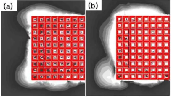
interface until they reach an edge where they can radiate. Surface waves for the spiral PBG structures with and without vias are examined by HFSS. The simulated surface waves are depicted in the Fig. 8. In these figures, electromagnetic radiation is leaked out to the radiation boxes outside of the PBG structures and waveguides. The electromagnetic radiation is stronger for the spiral PBG structures without vias than that with vias.
For the spiral PBG structures with vias, the energy of electromagnetic wave is less dissipated to the outside of the PBG structure (Fig. 8(a)) and thereby the energy of reflection wave is less decayed on the top plate surface, compared with the spiral PBG structures without vias (Fig. 8(b)).
This observation reveals that the vias play important roles in preventing the energy loss of
electromagnetic wave.
Fig. 7. Reflection phase of four different spiral PBG structures; the PBG structure given in Fig.
3(b) is named by the 4-turned spiral PBG structure Radiation at resonant frequency for the square PBG structures depicted in Fig. 3(c) was also
simulated for the comparison with the spiral PBG structure to see if the spiral metal shape in patch affects the radiation. Figure 9 shows simulated radiation patterns for the square PBG structures with vias (Fig. 9(a)) and without vias (Fig. 9(b)).
These simulated radiation patterns are close to those of the corresponding spiral PBG patterns, indicating that the spiral PBG structures proposed
in this study do not help in reducing the radiation.
Fig. 8. Radiation of electromagnetic waves on the
spiral PBG structures with vias (a) and without vias (b).
Fig. 9. Radiation of electromagnetic waves on the square PBG structure with vias (a) and without vias (b).
4. Summary
Reflection phases and radiation of the proposed PBG structures with the spiral metal patches were simulated by HFSS to characterize their performance. The resonant frequency of the proposed PBG structures gets significantly lower, as the length of the metal line elongates. The lowering of the resonant frequency is associated with the
increase in capacitance. And radiation pattern is nearly the same for the proposed PBG structures and the PBG structures with the square metal patches.
Acknowledgements
This work was supported by National R&D Project for Nano Science and Technology (10022916-2006-22), the Center for Integrated-Nano-Systems (CINS) of the Korea Research Foundation (KRF-2006-005-J03601),
"SystemIC2010" project of Korea Ministry of Commerce, Industry and Energy, the Korea Science and Engineering Foundation (KOSEF) through the
National Research Lab. Program
(R0A-2005-000-10045-02 (2007)), and the Nano R&D Program (M10703000980 -07M0300-98010).
References
[1] D. Sievenpiper, L. Zhang, R. F. J. Broas, N. G.
Alexopolous, and E. Yablonovitch, "High impedance electromagnetic surfaces with a forbidden frequency band", IEEE Trans. Microwave Theory and Tech., Vol.42, 1999, pp.2059-2074.
[2] M. Kim, J. B. Hacker, A. L. Sailer, S. Kim, D.
Sievenpiper and J. A. Higgins, "A rectangular TEM waveguide with photonic crystal walls for excitation of quasi-optical amplifiers", IEEE MTT-S International Microwave Symposium Digest, 1999, pp.543-546.
[3] F. R. Yang, K. P. Ma, Y. Qian and T. Itoh, "A novel TEM waveguide using uniplanar compact photonic-bandgap (UC-PBG) structure", IEEE Trans.
Microwave Theory and Tech., Vol.47, 1999, pp.2092-2098.
[4] Y. Qian, D. Sievenpiper, V. Radisic, E.
Yablonovitch, T. Itoh, "A novel approach for gain and bandwidth enhancement of patchantennas", in Proceedings of IEEE Radio and Wireless Conference, 1998, pp.221-224.
[5] F. R. Yang, K. P. Ma, Y. Qian and T. Itoh, "A uniplanar compact photonic-bandgap (UC-PBG) structure and its applications for microwave circuit", IEEE Trans. Microwave Theory and Tech., Vol.47,
1999, pp.1509-1514.
[6] J. -S. Lim, H. -S. Kim, J. -S. Park, D. Ahn and S. Nam, "A power amplifier with efficiency improved using defected ground structure", IEEE Microwave and Guided Wave Lett., Vol.11, 2001, pp.170-172.
[7] D. Sievenpiper, L. Zhang, E. Yablonovitch,“
High-impedance electromagnetic ground planes”, IEEE MTT-S International Microwave Symposium Digest, Vol.4, 1999 ,pp.1529-1532.
[8] E. I. Smirnova, A. S. Kesar, I. Mastovsky, M. A.
Shapiro, and R. J. Temkin, “Demonstration of a 17-GHz, High-Gradient Accelerator with a Photonic-Band-Gap Structure”,Phys. Rev. Lett., Vol.95, 2005, pp.074801.
[9] J. H. Wu, I. Shih, S. N. Qiu, and C. X. Qiu,
“Characterization of microwave photonic band-gap structures with bandpass filter applications”,J. Vac.
Sci. Technol.,Vol.24, 2006, pp.827-830.
[10] H. Lei, J. Chen, G. Nouet, S. Feng, Q. Gong, and X. Jiang, “Photonic band gap structures in the Thue-Morse lattice”, Phys. Rev. B, Vol.75, 2007, pp.205109.
[11] M. Rahman, and M. A. Stuchly, “Modeling and application of 2D photonic band gap structures”, in Proceedings of IEEE Aerospace Conference, Vol.2, 2001, pp.893.
BIOGRAPHY
Jho Wonjune (Member)
1995 : BS degree in Physics,Korea University.
2003 : MS degree in Micro Device Engineering, Korea University
~Present : Ph.D course in Biomicrosystem Engineering, KOREA, University
Yeom Donghyuk
2006 : BS degree in Electrical Engineering, Korea University
~Present : Master Course in Electrical Engineering, KOREA University
Yoon Changjoon
2005 : BS degree in Electrical Engineering, Korea University
~Present : Intergrated Master &
Ph.D Course in Electrical Engineering, KOREA University
Cho Kyoungah
1993 : BS degree in Chemistry, Sungshin Women's University 1995 : MS degree in Chemistry, Sungshin Women's University 2000: Ph.D degree in Chemistry, Tokyo University
~Present : Professor in Institute for Nano Science, KOREA University
Kim Sangsig
1985 : BS degree in Physics, Korea University.
1987 : MS degree in Physics, Korea University.
1990 : Ph.D degree in Physics, Columbia University
~Present : Professor in School of Electrical Engineering, KOREA University