• 검색 결과가 없습니다.

Criteria and Limitations for Power Rails Merging in a Power Distribution Network Design

N/A
N/A
Protected

Academic year: 2021

Share "Criteria and Limitations for Power Rails Merging in a Power Distribution Network Design"

Copied!
5
0
0

로드 중.... (전체 텍스트 보기)

전체 글

(1)

Criteria and Limitations for Power Rails Merging in a Power Distribution Network Design

Li Wern Chew

Intel Architecture Group (IAG), Intel Microelectonics (M) Sdn. Bhd. Bayan Lepas FIZ Phase 3, 11900 Penang, Malaysia.

(Received September 13, 2013: Corrected September 30, 2013: Accepted December 2, 2013)

Abstract: Modern electronic devices such as tablets and smartphones are getting more powerful and efficient. The demand in feature sets, functionality and usability increase exponentially and this has posed a great challenge to the design of a power distribution network (PDN). Power rails merging is a popular option used today in a PDN design as numerous power rails are no longer feasible due to form factor limitation and cost constraint. In this paper, the criteria and limitations for power rails merging are discussed. Despite having all the advantages such as pin count reduction, decoupling capacitors sharing, lower impedance and cost saving, power rails merging can however, introduce coupling noise to the system. In view of this, a PDN design with power rails merging that fulfills design recommendations and specifications such as noise target, power well placement, voltage supply values as well as power supply quadrant assignment is extremely important.

Keywords: Coupling noise, Impedance profile, Package design, Power distribution network, Power rails merging

1. Introduction

For over 40 years, the electronics industry has been striving to make new devices more compact and efficient.

Traditional computing devices as such desktop computers are gradually being replaced by Ultrabook, tablets and smartphones. These mobile devices are not only becoming more powerful and affordable, their performance in terms of feature sets, functionality and usability has increased exponentially. Typically, as feature sets increase, more power rails are needed in a power distribution network (PDN) design to support each of the functional blocks in a processor chip. Besides, high performance electronic devices that achieved breakthrough in processing capability usually consume more power.

As the trend of electronic systems design moves towards increased robustness, higher processing capability and faster processing speed, their design specifications such as form factor, power consumption and implementation cost on the other hand, are expected to trim down from one design phase to another. This has caused the PDN design to become one of the most critical design components in a highperformance system particularly in a system-on-chip design.
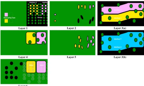
1-4)

Today, many PDNs are designed in such a way that two or more

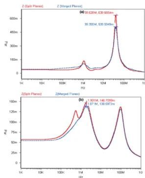
functional blocks in a processor chip share the same voltage supply source. With power rails merging, it enables decoupling capacitors sharing as well as embedded capacitance on the silicon. This not only helps in saving component cost and physical space but more capacitance can also dampen the impedance resonance peak. In addition, with a larger power plane, the resistance of the layout modeling is also expected to be lower since the resistance is inversely proportional to the area of the power plane. Thus, in general, the PDN with merged power rails is expected to perform better than the one with split power rails.

However, this might not be the case when noise coupling issue is taken into consideration. In a PDN design, some functional blocks especially those withhigh frequency input/

output (I/O) buffers would require independent power rails to minimize the coupling noise.

5)

Since there are some package design engineers who prefer to merge while there are others who choose to unmerge power rails in their PDN designs, the criteria and limitations for power rails merging are discussed in this paper. Section 2 first describes the power rails merging option. The advantages, criteria, and limitations for power rails merging are then presented in Section 3. Section 4 shows some simulation data in support of this study and finally, Section 5 concludes this paper.

Corresponding author

E-mail: [email protected]

© 2013, The Korean Microelectronics and Packaging Society

This is an Open-Access article distributed under the terms of the Creative Commons Attribution Non-Commercial License(http://creativecommons.org/

licenses/by-nc/3.0) which permits unrestricted non-commercial use, distribution, and reproduction in any medium, provided the original work is

properly cited.

(2)

In a PDN design, it is desirable to have a clean, undistorted power supply from the voltage source to each of the functional blocks for the smooth operation of the processor chip. The optimum design for such PDN is to provide a large individual power rail from the VRM to each of the functional blocks. However, often due to form factor limitation and cost constraint, individual power rail supply is usually not feasible in a real-world design. Thus, power rails merging is one of the common options used in most PDN designs where some functional blocks are designed to share the same power rail either from the package level or from the board level all the way to the pins of the chip.

Figure 1 and Figure 2 show the examples of a 6 layers PKG layout modeling. In these layout models, two functional blocks namely X and Y are considered. In layout model no. 1, Layer 3 and Layer 5 are the power and ground planes respectively. Both functional blocks X and Y can be supplied with the individual power rails (Layer 3a) or merged power rails (Layer 3b) at Layer 3 of the PKG model no. 1. For layout model no.2, Layer 2 and Layer 4 are the power and ground planes respectively while Layer 2a is the split power rails and Layer 2b is the merged power rails

that are connected to both the board and package substrates.

This not only allows form factor reduction in layout design due to the lesser number of power rails and power pins needed but additional passive components such as voltage regulator modules and bulk capacitors can also be eliminated. Consequently the hardware implementation cost of the platform is reduced.

In addition, power rails merging also allows the functional blocks involved to share the package or board decoupling capacitors as well as the embedded capacitance on the silicon module. These additional capacitances can help to dampen the resonance impedance of the PDN and reduce the transient noise of the functional circuits. Moreover, the power rails merger option creates a larger power plane in a PDN design. The resistance of the plane is also expected to be lower since resistance is inversely proportional to the area of the power plane. Thus, in general, the PDN with merged power rails is anticipated to outperform the one with split power rails.

3.2. Criteria

In power rails merging, the voltage planes for two or

Fig. 1. Layout modeling no. 1. Layer 3(a): Split power rails option. Layer 3(b): Merged power rails option.

(3)

more functional blocks are combined together and they all share one voltage source. Besides the need to have a similar voltage supply magnitude, it is also important to ensure that those power rails are from the same voltage quadrant. For example, in a PDN design, the board layout is usually divided into four quadrants: the north (<1.0V), south (1.0V- 1.4V), east (1.0V-2.0V) and west quadrants (>2.0V). Each of these quadrants has its own voltage supply range and it is generally more effective and simpler to merge power rails that are from the same voltage quadrant, especially due to physical routing concerns.

Another aspect to be considered before a power rails merger can be implemented is the power noise tolerance factor. This is because the merged power rails are assigned to the same power pins or balls on the package. Hence, the shared power rail and pin need to be designed carefully in order to meet the individual voltage drop and noise specification for all the power rails involved.

3.3. Limitations

Power rails merging in a PDN design is not always achievable and in fact, it is a challenging task for a layout designer. Besides ensuring that the power source placement is effective and making sure that the power planes meet the design recommendations such as plane length and width, routing gaps etc., the package or board layout design also needs to avoid having parallel power or signaling path routing between the substrate layers. This means that there should not be two or more power planes that are running in parallel between the substrate layers. Furthermore, certain design rules such as minimum gaps between signal and

power routes also need to be taken into consideration.

When two or more power rails are merged, the power rails will encounter additional coupling noise from the adjacent power rails that are being merged together. In view of this, power rails merging might not be advisable when noise coupling between one power rail to the other is taken into consideration.

6-8)

In

5)

, it has been shown that a PDN design with power plane merging is effective for functional blocks with current profile that has low frequency components or step function behavior. On the other hand, for functional blocks with a fast or a random switching pattern, it requires a PDN design with split power planes to provide a lower peak-to-peak noise.

4. Simulation Results and Discussion

The PDN performance is generally measured in terms of the impedance and transient noise profiles where they are in the frequency and time domains respectively. In a conventional design of PDNs, the impedance is required to be less than the target impedance over the frequency range of interest to minimize the voltage drop and to suppress the inductive noise during data transitions. Besides, transient analysis is also performed to ensure that the time-varying fluctuation of voltage that is caused by the current that flows through the PCB and PKG from the VRM to the processor chip does not cause reliability problems.

The evaluation of a PDN design with merged power rails is

carried out with the methodology or process presented in.

9)

In

this study, the package layout models presented in Figure 1

and Figure 2 are applied in the simulations. Here, the

Fig. 2. Layout modeling no. 2. Layer 2(a): Split power rails option. Layer 2(b): Merged power rails option.

(4)

voltage supply is set at 1.05V and two bulk capacitors of 22uF and package decoupling capacitors of 1uF are used.

The silicon module resistor and capacitor are 15 mΩ and 20nF respectively. SPICE simulation tool

10)

is then used to simulate the impedance profile of the PDN.

Table I(a) and Table I(b) shows the power pins and passive components needed in a PDN using layout model no. 1 and no. 2 respectively with split and merged power rails. It can be seen from the Table that with merged power rails, power pins/balls and passive components needed are much lesser. This will lead to a significant cost saving when a large amount of platform using the PDN design with merged power rails is manufactured.

4.1. Frequency Domain Analysis

Figure 3(a) and Figure 3(b) shows the impedance profiles comparison for both PDNs with split and merged power rails using layout model no. 1 and no. 2 respectively. From the simulation results, it can be seen that the impedance peak for layout model no. 1 is reduced by 130 mΩ for the PDN with merged power rails. For layout model no. 2, the low frequency inductance for PDN with merged power rails is dampened and the resonance peak is also reduced.

This shows that power rails merging can improve the PDN performance in terms of impedance value. This finding is correlated to the theoretical expectation.

With merged power rails, each of the functional blocks X and Y will have double the amount of decoupling capacitance as well as the embedded capacitance on the silicon modules, resulting in a lower impedance value.

4.2. Time Domain Analysis

The load current profile represents the transistor switching behavior and it is a plot of the current sourced or sunk over time. Here, four types of load current behaviors are taken into consideration. Figure 4(a) shows a load current with a Layout Model no. 2

Number of Functional Block X

Functional

Block Y Split rails Merged rails

Voltage source 1 1 2 1

Bulk capacitor 2 2 4 2

Package capacitor 0 1 1 1

Power pin/ball 1 1 2 1

Fig. 3. Impedance profiles comparison for the PDN with split and merged power rails option. (a) Layout model no. 1. (b) Layout model no. 2.

Fig. 4. Load current behaviors. (a) High frequency component, (b)

Low frequency component, (c) Step function behavior, (d)

Random pattern behavior.

(5)

fast switching cycle whereas Figure 4(b) shows a load current with a slower switching cycle. In Figure 4(c) and Figure 4(d), load currents with a step function and a random behavior respectively are presented. It should be noted that these load currents in the same set have the same maximum magnitude.

Table II and Table III show the peak-to-peak noise measurements at both functional blocks X and Y for the PDN using layout model no. 1 and no. 2 respectively with split and merged power rails option using the different types of load current behaviors. It can be seen from the simulation results that if both functional blocks X and Y have load currents with step function behavior or their transistors' switching frequency is slower, power rails merging can help to improve the peak-to-peak noise. However, coupling noises are generated when power rails are merged for interfaces that have load currents with high frequency contents or random switching pattern. Thus, under this situation, a PDN with split power rails would generally be preferred.

5. Conclusion

This paper presented the criteria and limitations for the power rails merger option in a PDN design. Power rails merging enables power pins count reduction, decoupling capacitors sharing and passive components reduction which leads to form factor reduction, lower PDN impedance peak and cost saving in hardware implementation. However, since power rails merging will introduce coupling noises into the system, careful consideration needs to be given to overcome this problem. Design specifications and recommendations such as noise target, power source placement, power supply values and quadrant assignment

are extremely important and they need to be captured during the PDN design.

References

1. M. Swaminathan, E. Engin, “Power Integrity Modeling and Design for Semiconductors and Systems”, Ed. 1, Prentice Hall Modern Semiconductor Design Series, Nov. (2007).

2. S. L. Huh and M. Swaminathan, “Are Power Planes Neces- sary for High Speed Signaling?”, DesignCon (2012). http://

www.esystemdesign.com/pdfs/

DesignCon2012_Are_Power_Planes_Necessary.pdf. Last accessed: 13 Feb. (2013).

3. B. Amelifard, M. Pedram, “Design of an efficient power delivery network in an soc to enable dynamic power man- agement”, ACM/IEEE International Symposium on Low Power Electronics and Design, pp.328-333, (2007).

4. C. Wang and etc., “An Efficient Approach for Power Delivery Network Design With Closed-Form Expressions for Parasitic Interconnect Inductances”, IEEE Transactions on Advanced Packaging, 29(2), (2006).

5. L. W. Chew, “Power plane merger option based on load cur- rent behaviours”, Proceeding of IEEE 17

th

Workshop on Sig- nal and Power Integrity, SPI, Paris, France, (2013).

6. M. Popovich and E. G. Friedman, “Noise coupling in multi- voltage power distribution systems with decoupling capaci- tors”, Proc. IEEE Int. Symp. Circuits Syst., I, 620 (2005).

7. J. L Knighten, B. Archambeault, J. Fan, et al., “PDN Design Strategies: I. Ceramic SMT Decoupling Capacitors? What Values Should I Choose?”, IEEE EMC Society Newslette, 34, (2005).

8. J. L Knighten, B. Archambeault, J. Fan, et al., “PDN Design Strategies: II. Ceramic SMT Decoupling Capacitors? Does Location Matter?”, IEEE EMC Society Newsletter, 207, 56 (2006).

9. L. W. Chew, “Design and Analysis of Power Delivery Net- work in a SoC: A Review”, Proceeding of International Con- ference on Electronics Packaging, ICEP, Apr. (2012).

10. Synopsys - SPICE Simulation Tool. http://www.synop-

sys.com/Tools/Verification/AMSVerification/CircuitSimula-

tion/HSPICE/Pages/default.aspx. Last accessed: Feb. 2013

수치

Figure 1 and Figure 2 show the examples of a 6 layers PKG layout modeling. In these layout models, two functional blocks namely X and Y are considered
Fig. 3. Impedance profiles comparison for the PDN with split and merged power rails option

참조

관련 문서

 Units of the average power are watts, while units of complex power are volt-amps(VA), and the units of reactive power are volt-amp reactive (VAR)... Complex Power in

Basic knowledge of fluid mechanics for hydropower, wave power, and wind power.. Basic physical

How to strengthening safety assessment capability for design and operation of nuclear power plants. ● Opening

Edit the layout in the design magazine, the nature of the design, the designers are trying to convey the power of the message depends on the magazine

Owing to nuclear power plant data characteristics such as nonlinear, time sequential and multivariate, in this light, this thesis aims at proposing an

In compact rectenna design, wireless power transmission technology is expected to be low power and low voltage in order to drive wireless

In this paper, we propose tree-based greedy algorithm to solve the minimum power broadcasting problem for minimizing the total transmit power on broadcasting in wireless

The front panel design may differ by chassis. A front panel module mainly consists of power switch, reset switch, power LED, hard drive activity LED, speaker and etc.