반도체디스플레이기술학회지 제18권 제4호(2019년 12월)
Journal of the Semiconductor & Display Technology, Vol. 18, No. 4. December 2019.
134
전하보유모델에 기초한 SONOS 플래시 메모리의 전하 저장층 두께에 따른 트랩 분석
송유민*· 정준교*· 성재영*· 이가원*†
*†충남대학교 전자공학과
Analysis of Trap Dependence on Charge Trapping Layer Thickness in SONOS Flash Memory Devices Based on Charge Retention Model
Yu-min Song*, Junkyo Jeong*, Jaeyoung Sung* and Ga-won Lee*†
*†Chungnam National University, Department of Electronics Engineering
ABSTRACT
In this paper, the data retention characteristics were analyzed to find out the thickness effect on the trap energy distribution of silicon nitride in the silicon-oxide-nitride-oxide-silicon (SONOS) flash memory devices. The nitride films were prepared by low pressure chemical vapor deposition (LPCVD). The flat band voltage shift in the programmed device was measured at the elevated temperatures to observe the thermal excitation of electrons from the nitride traps in the retention mode. The trap energy distribution was extracted using the charge decay rates and the experimental results show that the portion of the shallow interface trap in the total nitride trap amount including interface and bulk trap increases as the nitride thickness decreases.
Key Words : SONOS Flash memory, Trap density distribution, Charge retention, Charge-trapping layer, Film thickness
1. 서 론1
Silicon-Oxide-Nitride-Oxide-Silicon (SONOS) 플래시 메모리 는 저 전력 동작과 소자 축소의 용이성 및 종래의 CMOS 공정과의 호환성 등의 장점으로 비휘발성 메모리로 연구 되어 왔다 [1]. 최근 낸드 플래시 메모리의 경우 메모리 용량 집적화를 위해BiCS, pBiCs, TCAT 및 SMArT 구조와 같은 3D 구조와 함께 multi-level cell(MLC)와 triple-level cell(TLC)와 같은 기술들이 도입되고 있다 [2-9]. SONOS 유 형의 플래시메모리는 데이터를 실리콘질화막 (Si3N4)으로 구성된 전하저장층의 트랩에 저장하는 구조로 되어있다.
따라서 쓰기/읽기 속도, 데이터 보유 능력, 신뢰성과 같은 메모리 특성이 Si3N4 트랩의 에너지 레벨과 밀도 특성에 좌우된다 [10-12]. 전하저장층의 트랩 특성을 제어하기 위
†E-mail: [email protected]
해 Si3N4에 실리콘 나노크리스탈을 넣는 방법 등 다양한 방법이 시도되어 왔다 [13-15].
메모리 성능을 개선시키기 위해서는 트랩을 제어할 수 있는 공정 제안과 함께 트랩 특성을 밝힐 수 있는 분석법 의 개발도 매우 중요한데 Si3N4 트랩을 분석하기 위해 몇 가지 트랩 분석 방법이 제안되어 왔다 [16, 17]. 이에 본 연 구에서는 Charge Retention 특성에 기반한 트랩 분석 방법을 사용하여 전하저장층의 두께에 따른 트랩 밀도의 에너지 분포를 추출하였다.
2. 실 험
SONOS구조의 Capacitor소자를 제작하기 위해 prime 등 급의 p-type 실리콘 웨이퍼 위에 7 nm의 tunneling oxide (SiO2) 을 thermal oxidation 으로 형성하였다. 이 후 전자저장층의 두께에 따른 트랩밀도분포 변화를 분석하기 위해 Si3N4을
전하보유모델에 기초한 SONOS 플래시 메모리의 전하 저장층 두께에 따른 트랩 분석
Journal of KSDT Vol. 18, No. 4, 2019 135
low-pressure chemical deposition (LPCVD) 공정으로 7 nm, 15 nm, 20 nm 로 증착하였다. Blocking oxide는 15 nm의 LPCVD SiO2
박막을 사용하였고 Gate 형성을 위해 100 nm Ti 증착을 Sputter 공정으로 진행하였다.
전기적 특성은 Hewlett Packard 4282A LCR meter로 측정하 였다. Data retention 특성 분석은 프로그램된 소자의 100°C 에서의 flat band voltage shift (∆VFB) 를 측정하여 진행하였다.
(a)
(b)
Fig. 1. (a) Schematic diagram of SONOS capacitor-type device and (b) measurement results of electrical characteristics in the fabricated devices.
Fig. 1은 소자의 모식도와 제작된 소자의 초기 상태 (initial), program (PGM), erase (ERS) 특성을 Capacitance-Voltage 측정을 통해 보여준다.
3. 결과 및 고찰 3.1 Charge retention model
Si3N4 트랩을 추출하기 위해 프로그램을 진행한 후 100°C에서의 ∆VFB를 측정하였다. Data retention decay 특성으 로부터 에너지레벨에 대한 트랩 밀도는 Wang-White model [16, 17]에 따라 다음과 같은 식으로 추출하였다.
∆ ≅ 2.3 (1)
(2)
2 ∗ ∗ /
식 (1)과 식 (2)에서 ETA 는 Si3N4의 컨덕션 레벨로부터 트 랩의 에너지 레벨의 차이를 의미하며, 은 capture cross- section, ∗은 Si3N4 안에서 전자의 유효질량, h은 플랑크 상수를 의미한다.
3.2 Si3N4 두께에 따른 트랩 분포 추출 결과 Fig. 2는 위에서 기술한 charge retention model을 통해 추출 한 LPCVD Si3N4 의 트랩 분포를 보여준다. 박막의 두께에 따라 트랩의 양이 달라지기 때문에 각 조건에서 추출한 트랩 밀도를 최대값으로 정규화하여 비교하였다. Si3N4의 두께가 얇은 경우 보다 shallow 한 트랩의 양이 전체 트랩 의 양에서 차지하는 비중이 커짐을 확인할 수 있다.
Fig. 2. Extracted trap density according to the energy level of Si3N4 deposited by LPCVD. In the experiment, Si3N4 thickness is varied to 7 nm, 15 nm, and 20 nm.
3.3 Si3N4 트랩 분포 추출 결과 고찰
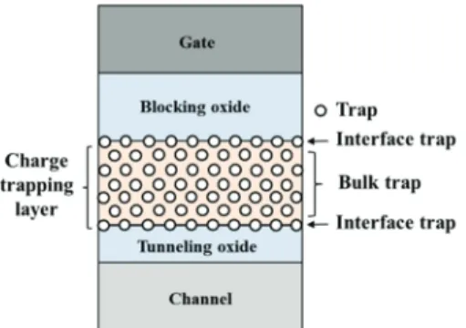
Fig. 3은 SONOS구조에서 charge trapping layer인 Si3N4의 트 랩을 도시한 그림으로 트랩의 위치에 따라 bulk trap과 interface trap트랩으로 나누었다. 위치에 따라 trap을 구분한 이유는 silicon nitride 형성 시 인접한 박막, 특히 산소가 다 량 함유된SiO2 박막의 존재에 따라 Fig. 4에 도시한 silicon nitride의 Si과 N 의 화학적 결합 상태가 달라질 수 있고 이 로 인해 생성되는 trap의 에너지 준위가 상이할 수 있기 때문이다. Si3N4의 band-gate state로 알려진 결함은 Si-N 결합 에서의 N vacancy인데 이 결함이 산소로 치환될 경우 에너
송유민 · 정준교 · 성재영 · 이가원
반도체디스플레이기술학회지 제18권 제4호, 2019 136
지 준위가 valence band와 conduction band 에 가깝게 위치하 고 있다고 보고되고 있다 [18-20]. 이는 산소와의 반응 가 능성이 높은 interface 영역에서 형성된 trap들의 에너지 준 위가 shallow 할 수 있음을 의미한다. 따라서 Si3N4박막이 얇아 bulk trap의 양이 총 trap의 양에서 차지하는 비중이 줄 게 되면 interface trap의 비중이 증가하면서 Fig. 3에 추출 된 결과와 같이 shallow trap 의 비중이 크게 나올 수 있 게 된다.
이러한 shallow trap은 같은 시간 동안 더 많은 데이터 손 실을 야기하기 때문에 신뢰성을 악화시키는 것으로 알려 져 있다. 따라서 추출된 결과는 Si3N4의 두께가 얇은 경우 메모리 특성 열화가 나타나는 기존의 결과들을 잘 설명 해준다고 할 수 있다.
Fig. 3. Schematic diagram of trap sites in the SONOS capacitor-type device.
(a) (b)
Fig. 4. (a) Tetrahedral unit of Si3N4 satisfying ideal stoichiometry and (b) solid Si3N4 film.
4. 결 론
SONOS 구조의 플래시 메모리 성능은 전하저장층인 Si3N4의 트랩 특성에 큰 영향을 받기 때문에 트랩의 밀도 와 에너지 준위 등을 정확하게 분석하는 것은 소자 개선 을 위해 매우 중요하다고 할 수 있다. 본 논문에서는 charge retention model을 기반으로 Si3N4두께에 따른 트랩의
에너지 분포를 추출하였다. Si3N4의 두께가 얇은 경우 (7nm) 총 트랩에서 shallow trap의 비중이 현저하게 증가하 는 것을 확인하였으며 이는 박막의 두께가 얇은 경우 Si3N4와 SiO2 계면에 존재하는 interface 트랩의 영향이 증가 되기 때문으로 판단된다. 향후 다양한 공정 조건 하에서 제작된 소자에 적용한다면 신뢰성을 포함한 소자 성능 향상에 기여할 수 있을 것으로 기대된다.
감사의 글
이 논문은 2019년도 정부(과학기술정보통신부)의 재원 으로 한국연구재단-나노·소재기술개발사업의 지원을 받 아 수행된 연구임 (2009-0082580). 또한 2019년도 정부(미래 창조과학부)의 재원으로 한국연구재단의 지원을 받아 수 행된 연구임 (NRF-2019R1A2C1084717).
참고문헌
1. French, M. L., Chen, C. Y., Sathianathan, H., &
White, M. H. “Design and scaling of a SONOS multidielectric device for nonvolatile memory applications”, IEEE Transactions on Components, Packaging, and Manufacturing Technology: Part A, 17(3), 390-397. (1994).
2. Tanaka, H., Kido, M., Yahashi, K., Oomura, M., Katsumata, R., Kito, M., ... & Iwata, Y. “Bit cost scalable technology with punch and plug process for ultra high density flash memory”, In 2007 IEEE Symposium on VLSI Technology pp. 14-15. IEEE.
(2007).
3. Katsumata, R., Kito, M., Fukuzumi, Y., Kido, M., Tanaka, H., Komori, Y., ... & Zhang, L. “Pipe-shaped BiCS flash memory with 16 stacked layers and multi- level-cell operation for ultra high density storage devices”, In 2009 Symposium on VLSI Technology pp.
136-137. IEEE. (2009).
4. Jang, J., Kim, H. S., Cho, W., Cho, H., Kim, J., Shim, S.
I., ... & Lim, J. S. “Vertical cell array using TCAT (Terabit Cell Array Transistor) technology for ultra high density NAND flash memory”, In 2009 Symposium on VLSI Technology pp. 192-193. IEEE. (2009).
5. Choi, E. S., & Park, S. K. “Device considerations for high density and highly reliable 3D NAND flash cell in near future”, In 2012 International Electron Devices Meeting pp. 9-4. IEEE. (2012).
6. Whang, S., Lee, K., Shin, D., Kim, B., Kim, M., Bin, J., ... & Cho, S. “Novel 3-dimensional dual control-gate with surrounding floating-gate (DC-SF) NAND flash
전하보유모델에 기초한 SONOS 플래시 메모리의 전하 저장층 두께에 따른 트랩 분석
Journal of KSDT Vol. 18, No. 4, 2019 137
cell for 1Tb file storage application”, In 2010 International Electron Devices Meeting pp. 29-7. IEEE.
(2010).
7. Kim, W., Choi, S., Sung, J., Lee, T., Park, C., Ko, H., ...
& Park, Y. “Multi-layered vertical gate NAND flash overcoming stacking limit for terabit density storage”, In 2009 Symposium on VLSI Technology pp. 188-189.
IEEE. (2009).
8. Ricco, B., Torelli, G., Lanzoni, M., Manstretta, A., Maes, H. E., Montanari, D., & Modelli, A. “Nonvolatile multilevel memories for digital applications”, Proceedings of the IEEE, 86(12), 2399-2423. (1998).
9. Bez, R., Camerlenghi, E., Modelli, A., & Visconti, A.
“Introduction to flash memory”, Proceedings of the IEEE, 91(4), 489-502. (2003).
10. White, M. H., Yang, Y., Purwar, A., & French, M. L. “A low voltage SONOS nonvolatile semiconductor memory technology”, IEEE Transactions on Components, Packaging, and Manufacturing Technology: Part A, 20(2), 190-195. (1997).
11. Arreghini, A., Akil, N., Driussi, F., Esseni, D., Selmi, L.,
& Van Duuren, M. J. “Long term charge retention dynamics of SONOS cells”, Solid-State Electronics, 52(9), 1460-1466. (2008).
12. Chang, J. J. “Theory of MNOS memory transistor”, IEEE Transactions on Electron Devices, 24(5), 511-518.
(1977).
13. Chiang, T. Y., Chao, T. S., Wu, Y. H., & Yang, W. L.
“High-program/erase-speed SONOS with in situ silicon nanocrystals”, IEEE Electron Device Letters, 29(10), 1148-1151. (2008).
14. Choi, S., Yang, H., Chang, M., Baek, S., Hwang, H., Jeon, S., ... & Kim, C. “Memory characteristics of
silicon nitride with silicon nanocrystals as a charge trapping layer of nonvolatile memory devices”, Applied Physics Letters, 86(25), 251901. (2005).
15. Lim, J. G., Yang, S. D., Yun, H. J., Jung, J. K., Park, J.
H., Lim, C., ... & Lee, G. W. “High performance SONOS flash memory with in-situ silicon nanocrystals embedded in silicon nitride charge trapping layer”, Solid-State Electronics, 140, 134-138. (2018).
16. White, M. H. “Charge retention of scaled SONOS nonvolatile memory devices at elevated temperatures”, Solid-State Electronics, 44(6), 949-958. (2000).
17. Wang, Y., & White, M. H. “An analytical retention model for SONOS nonvolatile memory devices in the excess electron state”, Solid-State Electronics, 49(1), 97- 107. (2005).
18. Morokov, Y. N., Novikov, Y. N., Gritsenko, V. A., &
Wong, H. “Two-fold coordinated nitrogen atom: an electron trap in MOS devices with silicon oxynitride as the gate dielectric”, Microelectronic engineering, 48(1- 4), 175-178. (1999).
19. Wong, H., & Gritsenko, V. A. “Defects in silicon oxynitride gate dielectric films”, Microelectronics Reliability, 42(4-5), 597-605. (2002).
20. Perera, R., Ikeda, A., Hattori, R., & Kuroki, Y. “Effects of post annealing on removal of defect states in silicon oxynitride films grown by oxidation of silicon substrates nitrided in inductively coupled nitrogen plasma”, Thin Solid Films, 423(2), 212-217. (2003).
접수일: 2019년 12월 23일, 심사일: 2019년 12월 26일, 게재확정일: 2019년 12월 27일