A SONOS device with a separated charge trapping layer for improvement of charge
injection
Jae-Hyuk Ahn, Dong-Il Moon, Seung-Won Ko, Chang-Hoon Kim, Jee-Yeon Kim, Moon-Seok Kim, Myeong-Lok Seol, Joon-Bae Moon, Ji-Min Choi, Jae-Sub Oh, Sung-Jin Choi, and Yang-Kyu Choi
Citation: AIP Advances 7, 035205 (2017); doi: 10.1063/1.4978322 View online: http://dx.doi.org/10.1063/1.4978322
View Table of Contents: http://aip.scitation.org/toc/adv/7/3
Published by the American Institute of Physics
Articles you may be interested in
Influence of thickness on crystallinity in wafer-scale GaTe nanolayers grown by molecular beam epitaxy
AIP Advances 7, 035113 (2017); 10.1063/1.4978776
Droplet ejection and sliding on a flapping film
AIP Advances 7, 035014 (2017); 10.1063/1.4979008
Ultra-fast charge carrier dynamics across the spectrum of an optical gain media based on InAs/AlGaInAs/InP quantum dots
AIP Advances 7, 035122 (2017); 10.1063/1.4979556
Ab initio molecular dynamics study of temperature and pressure-dependent infrared dielectric functions of liquid methanol
AIP Advances 7, 035115 (2017); 10.1063/1.4978899
Dynamic high pressure generation through plasma implosion driven by an intense laser pulse
AIP Advances 7, 035007 (2017); 10.1063/1.4975633
In silico modeling and investigation of self-heating effects in composite nano cantilever biosensors with integrated piezoresistors
A SONOS device with a separated charge trapping layer
for improvement of charge injection
Jae-Hyuk Ahn,1Dong-Il Moon,2Seung-Won Ko,2Chang-Hoon Kim,2 Jee-Yeon Kim,2Moon-Seok Kim,2Myeong-Lok Seol,2Joon-Bae Moon,2 Ji-Min Choi,2Jae-Sub Oh,3Sung-Jin Choi,4and Yang-Kyu Choi2,a 1Department of Electronic Engineering, Kwangwoon University, Seoul 01897, Korea 2School of Electrical Engineering, KAIST, 291 Daehak-ro, Daejeon 34141, Korea 3National Nanofab Center, 291 Daehak-ro, Daejeon 34141, Korea
4School of Electrical Engineering, Kookmin University, 77 Jeongneung-ro, Seongbuk-gu,
Seoul 02707, Korea
(Received 23 February 2017; accepted 24 February 2017; published online 8 March 2017)
A charge trapping layer that is separated from the primary gate dielectric is implemented on a FinFET SONOS structure. By virtue of the reduced effective oxide thickness of the primary gate dielectric, a strong gate-to-channel coupling is obtained and thus short-channel effects in the proposed device are effectively suppressed. Moreover, a high program/erase speed and a large shift in the thresh-old voltage are achieved due to the improved charge injection by the reduced effective oxide thickness. The proposed structure has potential for use in high speed flash memory. © 2017 Author(s). All article content, except where
other-wise noted, is licensed under a Creative Commons Attribution (CC BY) license (http://creativecommons.org/licenses/by/4.0/). [http://dx.doi.org/10.1063/1.4978322]
A silicon-oxide-nitride-oxide-silicon (SONOS)-type device is widely used as a memory cell in flash memory.1,2 The SONOS device has many advantages over the device with a floating gate structure due to its charge trapping layer.3 The discrete trapped-charge storage of the SONOS device resolves capacitive coupling issue between adjacent floating gates, and thin gate stacks lead to the improved electrostatic characteristics, which allow downscaling of memory cells. The simple process and improved reliability of the charge trapping layer enables the SONOS device to be applied in three-dimensional (3D) stacked structure for ultra-high density flash memory.4–7
To achieve high performance with fast program or erase characteristics, new structures for the SONOS device have been proposed with the analysis of the charge injection mechanism. Forma-tion of dopant-segregated Schottky-barrier on the source/drain increases program speed by the high efficiency of charge injection originating from sharp band bending at the source/drain.8 Use of a high-k dielectric layer as the blocking oxide of SONOS increases the E-field across the tunneling oxide, leading to fast erase speed.9 In a bandgap engineered (BE)-SONOS device, the tunneling oxide of SONOS is replaced by a BE ONO layer.10Efficient hole tunneling occurs under the high E-field due to the band offset of the BE ONO layer, which allows fast erase speed. In these SONOS structures for high-speed program/erase, the charge trapping layer should be inserted in the gate dielectrics and thus it is hard to reduce the effective oxide thickness (EOT) of the gate dielectric for obtaining a high gate-to-channel coupling. A new SONOS structure with a strong gate-to-channel coupling is needed to improve charge injection by E-field enhancement for fast program/erase characteristics.
In this work, we propose a new structure in which the charge trapping layer is separated from the primary gate dielectric, thereby reducing the EOT and enhancing the gate-to-channel coupling.
aAuthor to whom correspondence should be addressed. Electronic mail:[email protected]
035205-2 Ahn et al. AIP Advances 7, 035205 (2017)
FIG. 1. Process flow of the FinFET SONOS device. (a) Proposed device. (b) Control device. After gate patterning, oxide spacer is formed and S/D implantation is carried out. RTP and forming gas annealing are then executed.
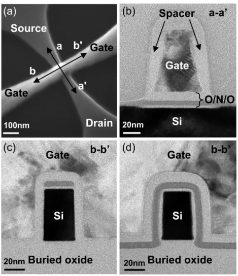
FIG. 2. (a) Tilted SEM image of the fabricated device. (b) TEM image along the a-a’ direction of (a). Thicknesses of the O/N/O layers for the charge storage node are 3 nm/5 nm/10 nm. (c) TEM image of the proposed device along the b-b’ direction. (d) TEM image of the control device along the b-b’ direction.
This structure is implemented on a FinFET device and its electrical characteristics are compared with those of a control device, i.e., a conventional FinFET SONOS device. The proposed structure shows the high gate-to-channel coupling verified by strong immunity to short-channel effects (SCEs) and the fast program/erase characteristics. Additionally, the analysis with TCAD simulation confirms that the reduced EOT at the fin sidewall increases the vertical E-field across the tunneling oxide to improve charge injection, resulting in the improved program/erase characteristics with high speed and low operation voltage.
A brief process flow for the proposed SONOS device is shown in Fig.1. A p-type (100) SOI wafer with a resistivity of 8.5–11.5 Ωcm, a top silicon thickness of 55 nm, and a buried oxide thickness of 145 nm was used as the starting material. As the first steps in the fabrication of the proposed device, a 3 nm-thick tunneling oxide was thermally grown, and a 5 nm-thick nitride was subsequently deposited as a charge trapping layer. After a fin was patterned, the charge trapping layer which was separated from the primary gate dielectric consequently remained on the top of the fin. Then, a 10 nm-thick blocking tetraethylorthosilicate (TEOS) oxide was deposited; thus, the thickness of the primary gate dielectric was equivalent to the thickness of the TEOS oxide because of conformal step coverage of the TEOS oxide. For further optimization, a very thin interfacial oxide should be thermally grown prior to the deposition of the blocking TEOS oxide. It is also expected that such an extremely thin interfacial oxide will not sacrifice the reduced EOT in the proposed device but will further improve the interface property. For a control device, a fin without the aforementioned tunneling oxide or charge trapping nitride was first patterned. Second, oxide/nitride/oxide (ONO) was sequentially deposited as a gate dielectric. Thus, the charge trapping layer conformally wrapped the fin, and the EOT of the control device was thicker than that of the proposed device. For both devices, an n+in situ doped poly-crystalline silicon (poly-Si) was deposited as a gate electrode, and
chemical mechanical polishing (CMP) was applied for the gate planarization. After the gate and spacer patterning, source/drain (S/D) implantation (arsenic, energy of 30 keV and a dose of 5×1015 cm-2), RTP annealing (1000◦C, 5 sec), and forming gas annealing (N2:H2=10:1, 400◦C, 30 min) were subsequently carried out. For the scaling of the gate stack with a more thinned blocking oxide,
FIG. 3. (a) Transfer characteristics of the fabricated devices. (b) Threshold voltages (VT), (c) subthreshold swing (SS), and (d)
035205-4 Ahn et al. AIP Advances 7, 035205 (2017)
it is necessary to utilize a high workfunction material as a gate electrode such as metal gate11 and p+ Poly-Si,12etc. The scanning electron microscopy (SEM) image in Fig.2 (a)shows the fabricated device after all process steps were completed. As shown in Fig.2 (b), the cross-sectional transmission electron microscopy (TEM) image of the fabricated device along the fin direction indicates that the nominal gate length of the fabricated devices is 50 nm, and the thicknesses of the deposited ONO layers are 3 nm, 5 nm, and 10 nm. Cross-sectional TEM images of the proposed device and the control device along the gate direction are shown in Figs.2(c)and(d), respectively. The charge trapping layers in both devices have the same thickness but the overall structures of the gate dielectric stacks notably differ.
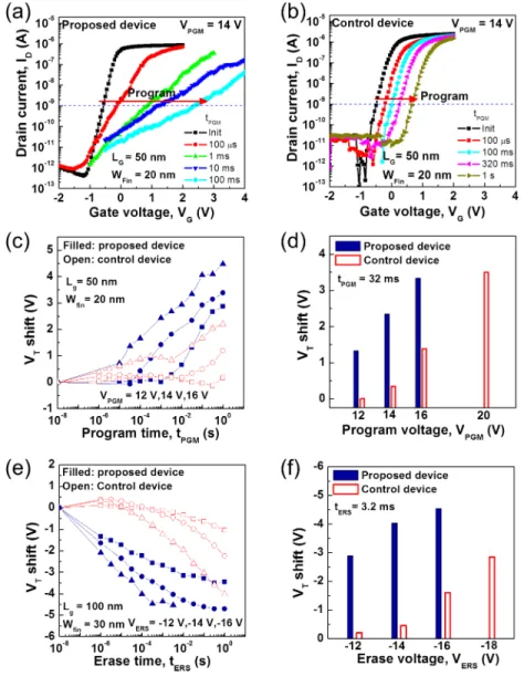
Figure3(a)shows the ID-VGtransfer characteristics of the fabricated devices. As indicators for the SCEs, the threshold voltage (VT), subthreshold swing (SS), and drain-induced barrier lowering (DIBL) are plotted in Figs.3 (b),(c), and(d)for various dimensions, respectively. For all the various dimensions, the SCEs are effectively suppressed in the proposed device with lower values of VT
FIG. 4. (a, b) Transfer characteristics of the proposed device and the control device by various program voltages. (c) Program transient characteristics under various program voltages. Faster program is observed in the proposed device. (d) Program voltage dependence on the VTshift. Program with low voltage is enabled in the proposed device. (e) Erase transient characteristics
under various erase voltages. Faster erase is shown in the proposed device. (f) Erase voltage dependence on the VTshift. Erase
roll-off, SS, and DIBL than those of the control device. These results are originated from a higher gate-to-channel coupling due to a lower EOT value at the fin sidewall of the proposed device than that of the control device.
Figures4 (a)and(b)show program characteristics of the proposed device and control devices, respectively. The Fowler–Nordheim (FN) tunneling method is used by application of the zero bias to the source/drain and the program voltage to the gate. The transfer characteristics of both devices are shifted to the right during the programming. This confirms that the ONO layer works normally as the charging trapping layer. Whereas a parallel shift of the transfer characteristics is observed in the control device, the SS of the proposed device is increased due to the programming. This change of the SS in the proposed device is caused by the structural difference compared to the control device. The proposed device can be referred to as two parallel transistors: a top transistor with an ONO layer and a sidewall transistor without an ONO layer. At program state, the VT of the top
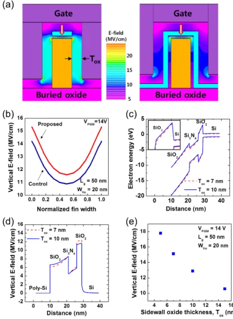
FIG. 5. (a) Cross-sectional E-field using 3-D TCAD simulation. (b) Vertical E-field inside the tunneling oxide is extracted along the dashed line in (a). The proposed device has a higher vertical E-field, which is used for the FN program. (c) Energy band diagram along the center of the fin. (d) Vertical E-field inside along the center of the fin. (e) Vertical E-field inside the tunneling oxide as a function of the primary gate oxide thickness at the fin sidewall. The vertical E-field is defined as an average value along the width direction at 1 nm above the silicon surface. A program voltage of 14 V is used for all the simulations.
035205-6 Ahn et al. AIP Advances 7, 035205 (2017)
transistor is increased but the VTof the sidewall transistor is constant, which results in the increased total value of the SS instead of a parallel shift of the VT. Despite the drawback that the high SS characteristics are not suitable for multi-level cell memory, the proposed device has the distinctive advantage of the improved charge injection for use in high speed flash memory, which will be discussed below.
Figure 4 (c)shows the program characteristics of the fabricated device at various bias con-ditions. Under the same program voltage conditions, the proposed device shows faster program characteristics than the control device. As observed in the VT shifts according to the program voltages in Fig. 4 (d), the program characteristics of the proposed device are better than those of the control device. In particular, a program voltage of 20 V is necessary to obtain the same VT shift at a program time of 32 ms in the control device, whereas a lower program voltage of 16 V is required in the proposed device. Figures 4 (e) and(f) show the erase characteristics of the fabricated devices. The programmed data is erased using the FN tunneling method. Sim-ilar to the trend observed in the program characteristics, the proposed device shows faster erase characteristics than the control device. Thus, erase with low voltage is achieved in the proposed device.
The fast program/erase characteristics and the low program/erase voltage of the proposed device were verified by a 3-D TCAD simulation13 with the same dimensions as those of the
fabricated devices. Figure 5 (a) shows the cross-sectional E-field for the proposed and control devices. As shown in Fig. 5 (b), the vertical E-field inside the tunneling oxide is strengthened in the proposed structure. We confirmed that the enhancement of the E-field is caused by the reduced EOT at the fin sidewall. Figure 5 (c) shows that downward band bending occurs due to the sidewall gates and the amount of band bending is increased as the thickness of the sidewall oxide is reduced. As shown in Figs. 5 (c)and(d), thinner primary gate oxide makes the energy band of the tunneling oxide steeper; the vertical field inside the tunneling oxide is enhanced. This result is verified in Fig. 5 (e), which shows that the vertical E-field increases as the primary gate oxide thickness is reduced. Therefore, this enhancement of the E-field boosts FN tunneling. It is concluded that the improved program/erase performance in the proposed device stems from the lowered EOT.
In conclusion, we demonstrated a FinFET SONOS device to improve charge injection with a separated charge trapping layer from the gate dielectric at the fin sidewall. The increased gate-to-channel coupling by the reduced EOT value at the fin sidewall not only suppressed the SCEs but also strengthened the vertical E-field inside the tunneling oxide to improve charge injection. The program/erase characteristics were enhanced with high speed and low operation voltage. Although further characterization and improvement of the device performance such as endurance and retention seem to be necessary, the new SONOS structure presented here will be used to design high speed flash memory.
ACKNOWLEDGMENTS
This work was sponsored in part by the Center for Integrated Smart Sensors funded by the Ministry of Education, Science and Technology as Global Frontier Project under Grant CISS-2011-0031848, by the IT R&D program of MKE/KEIT under Grant 10035320 (Development of novel 3D stacked devices and core materials for the next generation flash memory), by the Samsung Electronics Company Ltd., and by the SK Hynix Semiconductor Inc. The present research has been partially conducted by the Research Grant of Kwangwoon University in 2016.
1M. H. White, D. A. Adams, and J. Bu,IEEE Circuits and Devices Mag.16, 22 (2000). 2K. Kim, in IEDM Tech. Dig., 2005, pp. 323–326.
3J.-D. Lee, S.-H. Hur, and J.-D. Choi,IEEE Electron Device Lett.23, 264 (2002).
4H. Tanaka, M. Kido, K. Yahashi, M. Oomura, R. Katsumata, M. Kito, Y. Fukuzumi, M. Sato, Y. Nagata, and Y. Matsuoka,
in Symp. VLSI Technol. Dig., 2007, pp. 14–15.
5R. Katsumata, M. Kito, Y. Fukuzumi, M. Kido, H. Tanaka, Y. Komori, M. Ishiduki, J. Matsunami, T. Fujiwara, and Y. Nagata,
in Symp. VLSI Technol. Dig., 2009, pp. 136–137.
6J. Jang, H.-S. Kim, W. Cho, H. Cho, J. Kim, S. I. Shim, Y. Jang, J.-H. Jeong, B.-K. Son, and D. W. Kim, in Symp. VLSI
7H.-T. Lue, T.-H. Hsu, Y.-H. Hsiao, S. P. Hong, M. T. Wu, F. H. Hsu, N. Z. Lien, S.-Y. Wang, J.-Y. Hsieh, and L.-W. Yang,
in Symp. VLSI Technol. Dig., 2010, pp. 131–132.
8S.-J. Choi, J.-W. Han, S. Kim, M.-G. Jang, J. S. Kim, K. H. Kim, G. S. Lee, J. S. Oh, M. H. Song, and Y. C. Park,IEEE
Electron Device Lett.30, 78 (2009).
9C.-H. Lee, S.-H. Hur, Y.-C. Shin, J.-H. Choi, D.-G. Park, and K. Kim,Appl. Phys. Lett.86, 152908 (2005).
10T.-H. Hsu, H. T. Lue, Y.-C. King, J.-Y. Hsieh, E.-K. Lai, K.-Y. Hsieh, R. Liu, and C.-Y. Lu,IEEE Electron Device Lett.28,
443 (2007).
11S. Jeon, J. H. Han, J. H. Lee, S. Choi, H. Hwang, and C. Kim,IEEE Trans. Electron Devices52, 2654 (2005).
12M. H. White, Y. Yang, A. Purwar, and M. L. French,IEEE Trans. Compon., Packag. Manuf. Technol., Part A20, 190 (1997). 13Atlas User’s Manual: Device Simulation Software, SILVACO Int., Santa Clara, CA, 2008.