저전력 휴대용 통신단말을 위한 이온빔 처리된 HfO 2 박막의 특성 연구
김원배*, 이호영**
Study of Properties of HfO
2thin film for Low Power Mobile Information Device
Won Bae Kim*, Ho Young Lee**
요 약
본 연구에서는 이온빔 처리된 HfO2 박막을 이용한 액정디스플레이의 프리틸트각을 제어함으로써, 작은 구동전압에서도 안정적으로 구동할 수 있는 디스플레이 소자에 응용할 수 있는 특성을 연구하였다. HfO2 박막의 원자 수준의 증착을 통해서 높은 유전율의 박막 을 제조할 수 있었으며, 이는 저전력 구동을 위해서 필수적인 요소라고 생각한다. 또한 이러한 HfO2 박막의 액정배향성을 확인하여 균일한 액정배향을 통해서 디스플레이 소자로의 응용가능성을 확인하였다. 특히 HfO2 박막에서의 액정배향성에 대해서 액정배향의 대표적인 특성인 프리틸트각의 제어를 실험을 통해서 확인하였다. 실험결과 이온빔처리를 한 HfO2 박막에서의 액정배향의 특성을 접촉각특성을 대표화하여 정량화 할 수 있었다. 본 연구의 결과 액정의 배향성 확보 및 프리틸트각을 제어할 수 있는 고유전율 HfO2 박막의 제조가 가능한 것을 확인할 수 있었으며, 고유전율 특성에서 기인하는 저전력 구동의 가능성을 확인할 수 있었다.
Key Words : HfO2 ultrathin film, Liquid Crystal Display, High-k materials, Low driving voltage, pretilt angle
ABSTRACT
Ion-beam irradiation(IB) on HfO2 surface induced high-performance liquidcrystal(LC) driving at a 1-V threshold with vertical alignment of liquid crystals(LC). The high-k materials Atomic layer deposition was used to obtain LC orientation on ultrathin and high-quality films of HfO2 layers. To analyze surface morphological transition of HfO2 which can act as physical alignment effect of LC, atomic force microscopy images are employed with various IB intensities. The contact angle was measured to elucidate the mechanism of vertical alignment of LC on HfO2 with IB irradiation. Contact angle measurement show the surface energy changes via IB intensity increasing.
*송원대학교 전기전자공학과
**초당대학교 정보통신공학과
접수일자 : 2015년 8월 13일, 수정완료일자 : 2015년 9월 1일, 최종게재확정일자 : 2015년 9월 10일
I. Introduction
The uniformly aligned liquid crystal (LC) molecules on a polyimide (PI) is an important factor in the manufacture of LC displays (LCDs). Mechanical rubbing is the industry standard process for achieve this [1-4]. A PI layer with an anisotropic surface [5-8] which can create a pretilt angle between liquid crystal and its surface is essential for operating the LCDs with optically transparent and chemically stable insulating characteristics [9]. However, the rubbing process for LC alignment has major demerits
such as debris generation, local defects, and electrostatic discharge [10-11]. To decrease these defects, a cleaning process which slows down the manufacturing process and reduces its cost effectiveness have to be required in rubbing process. Also, the quality of the displays produced is degraded during the rubbing process. Over the past several years, several alternative alignment techniques have been investigated for inducing anisotropy on LC alignment layer surfaces by noncontact method [12]
including oblique deposition [13], plasma treatment [14], photoalignment [10], and nanostructured alignment
surfaces [9,10]. Above all, ion beam (IB) bombardment is a noncontact alignment method that provides reliability, controllability, a continuous manufacturing process, and high resolution displays. Depending on these non-contact alignment methods, many optically transparent insulators such as diamondlike carbon [15], SiC [16], SiOx[17], SiNx[18], γ-Fe2O5[5] have been reported as potential candidates for inorganic alignment materials. Even so, LC orientation on a brand new material with upgraded capacity is required to produce high-performance displays.
Many inorganic materials with high permittivities can reduce the voltage losses due to the LC alignment layers that are a trade-off for its capacitance. The lower voltage for LC operation can be applied to the LC under low external voltage by using high-k materials. This means that low power operation for LCD applications can be accomplished using a high-k alignment structure where the LC can be operatied effectively with a low threshold voltage. In this reasons, it has been intensively investigated in our previous work with optically transparent high-k insulating inorganic materials such as Al2O3[19], Ta2O5[11] and HfO2[20] for LCD sapplications.
The LC alignment mechanism is explained by a random network model of the atomic arrangement in the inorganic films surface. However, despite many efforts to find a simple low-cost method and different alignment materials, the LC orientation mechanism by IB bombardment is still not completely revealed. In our previous work, we reported a technique for the homogeneous alignment of LCDs on IB bombarded Ta2O5, and showed the mechanism that the creation of the pretilt angle was due to the IB bombardment breaking Ta-O and O-Ta bonds. The orientational order was thus generated by directional IB[11].
Among the many other potential high-k materials, HfO2
is considered as one of the most promising materials to satisfy considerably large band gap(5.68eV), high dielectric constant(k~30). In particular, IB bombarded LC alignment layers grown by atomic layer deposition(ALD) was studied in our group which reported that the non-stoichiometric HfO2 surface transformed to fully oxidized HfO2 by ion-bombardment The IB bombardment might induce activation of Hf dangling bonds on the film surface, which can easily be transformed to Hf-O bonding by supplying atmospheric oxygen. The strong van der Waals interactions between the HfO2 surfaces and LC molecules, which are more effective than LC molecular interactions,
are thought to have induced a random LC alignment before IB bombardment. When HfO2 surfaces were stabilized with ion bombardment to induce surface oxidization, the van der Waals interactions between HfO2 and LC decreased to a smaller value that was sufficiently weak to make a good balance with LC molecular interactions for vertical alignment[20]. In this study, we investigated about physical alignment effect and the thermal stabilities on HfO2 surface which is modified by IB bombardment. This is the series of our experiments about ultra thin HfO2 as a vertical alignment layers. Based on the chemical structure transition of HfO2 surface by IB bombardment revealed in our previous work, we studied on the topological transformation and wetting property analysis which is major tools for understanding of inorganic LC alignment layers. Also, we conducted thermal stability test which is important factor of LCDs reliabilities.
Ⅱ. Experimental
HfO2 thin films 10nm thick were deposited on the ITO-coated glass substrates via ALD using trimethylaluminum[Al(CH3)3] and water at a deposition temperature of 300°C. The films 10nm thick were exposed to Ar+ IB plasma with dosages of 1014-1015 ions/cm2 at an incident angle of 45 degree from the surface normal for 2 min at various energy intensities 0eV, 600eV, 1000eV, 1500eV, 2400eV, 3000eV. A current density in a beam of positive charged particles measures from a Faraday cup system was 3.7mA/cm2 and a plasma ion density measured by the double Langmuir probe tips was of approximately 1011cm-3.
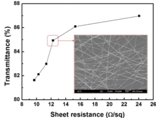
Figure 1. Plot of average transmittance versus sheet- esistance(Rs) for the Ag NW network films.
Inset is a FESEM image of Rs≈11.3Ω/sq Ag NW networks on glass substrate
As illustrated in figure 1, the IB system used to align the LC molecules in this study was based on a direct-current DuoPIGatron-type gun with a hot-filament ion source. The glass substrates with the HfO2 layer on the ITO electrodes were assembled in an anti-parallel configuration with a cell gap of 60μm to observe the pretilt angles, and VA-LCDs were prepared with a cell gap of 5μ m to examine the voltage-transmittance analysis. The cells were then filled with negative LCs (MJ98468; Merck) with a dielectric anisotropy (∆ε) of -4; refractive indices in the ordinary and extraordinary axes of 1.4742 and 1.5512, respectively; and and isotropic transition temperature of 75°C. The surface morphology of the samples was observed by atomic force microscopy (AFM) before (0 eV) and after (600 eV, 2400 eV) IB bombardment which can explain the possible LC alignment behavior.
The contact angle of each surface was measured by the sessile drop technique with de-ionized water using a Phoenix 300 surface angle analyzer(SEO) and analyzed with IMAGE PRO 300 software. Then the fabricated LC cells were put on the hot plate for the thermalstability test.
The temperature of the hot plate was changed from 50°C to 250°C with the increment of 50°C. Then, each LC cell was observed by the polarized optical microscope.
Ⅲ. Results and Discussion
Contact angle measurement can be considered a gauge of the relationship between liquid and the surface characteristics of a solid on which the liquid is placed.
Figure 2 shows the variation in contact angle on the HfO2/ITO films for various IB intensities at an incident angle of 45 degree and an exposure time of 2 min. The measured contact angleis 70, 53.8, 50.5, 50.5, 43.3, 50.5 degree with the incident IB intensity of 0 (beforeIBbombardment), 600, 1000, 1500, 2400 and 3000eV, respectively. From this result, we can confirm that the measured contact angle decreases with IB bombardment which means that the surface energy is increasing.
Furthermore, the films lost their hydrophobicity with increasing IB bombardment. We can also obtain the measured value of 50.5 degree which is limited contact angle for vertical alignment of LC molecules on the IB bombarded HfO2 surface.
To elucidate the physical alignment effect of LC on HfO2 surface, we employed AFM analysis which can
reveal the morphological transition on the HfO2 surface by IB bombardment.
Figure 2. Photomicrographs of the LC cells fabricated by PI/AgNW networks substrates (a) before and (b) after rubbing treatment under the crossed and parallel Nichols (A: analyzer, P: polarizer).
Figure 3. Transmittance versus incident angle of the LC molecules on the LC cell fabricated by PI/AgNW networks substrates, as measured by the crystal rotation method to obtain the pretilt angle.
(simulated curve in blue and experimental curve in red).
In the previous work at the same experimental conditions, there are random LC orientations with the IB intensity of 0eV and 600eV which has the rms roughness of under 5.5 nm. However, when the IB intensity increases, the rms roughness is increasing over 5.5nm which is suitable for good LC alignment states. From this result, it is found that the surface topological transition is progressed with IB bombardment and the minimum value of surface rms roughness is existing which is essential for vertical alignment of LC molecules as an physical alignment effect. As the contact angle is also related to the surface morphology, it can be thought that the increased rms roughness of HfO2 nano-structure increases the surface energy of HfO2 which can be detected by contact angle decreasing. This series of nano-structure related
surface energy variations can be considered as physical alignment factor which contributes to vertical alignment of LCs.
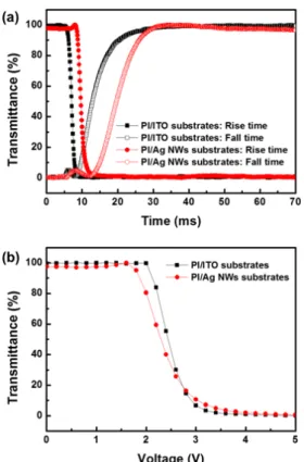
Figure 4. (a) RT curve and (b) V-T curves for the rubbing-aligned LC cells using ITO films and AgNW networks.
Figure 3 show the voltage-transmittance curve of HfO2
based VA-LCDs. The ion energy intensity, incident angle, and exposure time were 2400eV, 45 degree, and 120s, respectively. (We did same experiments again for confirm the reliability of our previous work.) The performance of existing VA-LCDs on IB bombarded PI is shown for comparison. The superior performance of V-T characteristics obtained with threshold voltage of 1V while the IB bombarded PI based VA-LCDs had the threshold voltage of 3.3V. The capacity of 10nm thick alignment layer is one of the most reasonable factor for explaining this result. The total capacitance can be expressed in simplified form as a linear combination of the alignment layer capacitance and the LC capacitance. The high-k HfO2 alignment layers can dramatically increase the capacitance of alignment layers which can reduce voltage losses due to LC alignment layers. Also, the thickness of HfO2 can be anotherr factor of increasing the capacitance of LC alignment layers. The 10nm thick alignment layers by ALD can reduce the alignment layer related voltage
losses. From this result, we can concluded that HfO2 based VA-LCDs can drop the threshold voltage which is essential for the low power operation of device.
Moreover, the thermal stability of the HfO2 based LC cells were examined. Thermal stability is one of the best merits of the inorganic alignment layer because the organic alignment layer results in a change of the pretilt angle and alteration of electrooptical properties due to its deterioration by thermal stress and does not secure a long life time. To evaluate the thermal stability in the HfO2
layers, the LC cells were exposed to high temperatures.
As seen in Figure 4, the HfO2 alignment layers did not deteriorateat high temperatures owing to robust properties of the inorganic materials. Eventually, they showed stable alignment properties, which secured the long life time of the advanced LCDs.
Ⅳ. Conclusion
In summary, VA-LCDs based on HfO2 layers with IB bombardment were embodied in this work. The 10 nm ultra-thin alignment layers were deposited by ALD process which can suppress the voltage losses due to the capacitance of thick LC alignment layers. The IB bombardment can induce the certain surface states of nano-structure which can vertically align the LC molecules. The nano-structure variation by IB bombardment can change the surface energy which is related to the vertical alignment of LCs. The HfO2 based VA-LCDs have merits of low power operation and stability under harsh conditions such as high temperatures.
References
[1] Y. J. Kim, Z. Zhuang, and J. S. Patel, Appl. Phys. Lett. 77, 513 (2000).
[2] M. F. Toney, T. P. Russell, J. A. Logan, H. Kikuchi, J. M.
Sands, and S. K. Kumer, Nature (London) 374, 709 (1995).
[3] C. Y. Huang, C. H. Lin, J. R. Wang, C. W. Huang, M. S.
Tsai, and A. Y. G. Fuh, J. Appl. Phys. 92, 7231 (2002).
[4] J. Hoogboom, T. Rasing, A. E. Rowan, and R. J. M. Nolte, J. Mater. Chem. 16, 1305 (2006).
[5] H. Y. Wu and R. P. Pan, Appl. Phy. Lett. 91, 074102 (2007).
[6] P. Chaudhari, J. A. Lacey, S. C. A. Lien, and J. L. Speidell, Jpn. J. Appl. Phys., Part2 37, L55 (1998).
[7] J. M. Geary, J. W. Goodgy, A. R. Kmetz, and J. S. Patel, J.
Appl. Phys. 62, 4100 (1987).
[8] J. H. Kim and C. Rosenblatt, J. Appl. Phys. 87, 155 (2000).
[9] F. S Yeung, J. Y. Ho, Y. W. Li, F. C. Xie, O. K. Tsui, P.
Sheng, and H. S. Kwok, Appl. Phys. Lett. 88, 051910 (2006).
[10] J. B. Kim, J. R. Lim, J. S. Park, H. J. Ahn, M. J. Lee, S.
J. Jo, M. Kim, D. Kang, S. J. Lee, Y. S. Kim, and H. K. Baik, Adv. Funct. Mater. 18, 1340 (2008).
[11] J. Y. Kim, B. Y. Oh, B. Y. Kim, Y. H. Kim, J. W. Han, J.
M. Han, and D. –S. Seo, Appl. Phy. Lett. 92, 043505 (2008).
[12] J. Y. L. Ho, V. G. Chigrinov, and H. S. Kwok, Appl. Phys.
Lett. 90, 243506 (2007).
[13] M. Lu, Jpn. J. Appl. Phys., Part1 43, 8156 (2004).
[14] C. Y. Lee, Y. L. Liu, K. Yi. Wu, M. Y. Chen, and J. C.
Hwang, Jpn. J. Appl. Phys. 47, 226 (2008).
[15] J. H. Choi, M. H. Ham, B. Y. Oh, J. Y. Hwang, S. H. Choi, D. –S. Seo, and J. M. Myoung, Liq. Cryst. 33, 947 (2006).
[16] J. B. Kim, K. C. Kim, H. J. Ahn, B. H. Hwang, D. C. Hyun, and H. K. Baik, Appl. Phys. Lett. 90, 043515 (2007).
[17] J. L. Janning, Appl. Phys. Lett. 21, 173 (1972).
[18] S. K. Lee, J. H. Kim, B. Y. Oh, D. H. Kang, B. Y. Kim, J.
W. Han, Y. H. Kim, J. M. Han, J. Y. Hwang, C. H. Ok, and D.-S. Seo, Jpn. J. Appl. Phys., Part1 46, 7711 (2007).
[19] H. G. Park, Y. H. Kim, B. Y. Ph, W. K. Lee, B. Y. Kim, D.-S. Seo, Appl. Phys. Lett. 93, 233507 (2008).
[20] W. K. Lee, B. Y. Oh, J. H. Lim, H. G. Park, B. Y. Kim, H.
J. Na, and D.-S. Seo, Appl. Phys. Lett. 94, 223507 (2009).
저자
김 원 배(Wonbae Kim) 정회원
․1982년 2월 : 조선대학교 전자공학과 학사졸업
․1989년 2월 : 조선대학교 컴퓨터공학과 석사졸업
․1995년 2월 : 조선대학교 전기공학과 박사졸업
․1993년 ∼ 현재 : 송원대학교 전기전자공학과 교수 <관심분야> : 우주공학, 위성통신, 마이크로프로세스
이 호 영(Hoyoung Lee) 정회원
․1988년 2월 : 조선대학교 전산기공학 과 학사
․1995년 8월 : 조선대학교 대학원 컴퓨 터공학과 석사
․2000년 2월 : 조선대학교 대학원 컴퓨 터공학과 박사
․2000년 3월 ∼ 현재 : 초당대학교 정보통신공학과 부교수 <관심분야> : 컴퓨터시스템, 네트워크, 유비쿼터스, LCD 기술