P2-103 / J. Lee
IMID 2009 DIGEST •
Abstract
Polymer solar cells were fabricated with gravure printing process and the effect of thermal annealing of gravure printed organic layer was investigated. The layer structure of polymer solar cells is glass / ITO / hole transfer layer / active layer / Al structure was fabricated. For the active layer, 1:1 ratio of poly-3-hexylthiophene (P3HT) and [6,6]-phenyl C61-butyric acid methyl ester (PCBM) mixture was applied. The P3HT/PCBM blend was gravure printed onto the substrates. The effect of thermal annealing was investigated by changing annealing time and the number of printing. Maximum 3.6% of power conversion efficiency was achieved with gravure printing of organic layer and thermal annealing in this work.
1. Introduction
Polymer solar cells have recently demonstrated 6% power conversion efficiency (PCE). Even though it has lower efficiency than inorganic solar cells, polymer solar cells are getting attention due to its low cost by simple fabrication processes. Polymer solar cells have the advantage of light weight and compactness. For the commercialization of polymer solar cells, development of printing process is required. Gravure printing process is known to have high throughput and relatively high resolution.
In this work we developed gravure printing process of organic thin films for polymer process. Polymer solar cells were fabricated with gravure printing process and the effect of thermal annealing of gravure printed organic layer was investigated.
2. Experimental
The layer structure of polymer solar cells is glass / ITO / hole transfer layer / active layer / Al structure was fabricated. Poly(3,4-ethylenedioxythiophene (PEDOT): poly (styrenesulfonate) (PSS)layer was formed as hole transfer layer. For the active layer, 1:1 ratio of poly-3-hexylthiophene (P3HT) and [6,6]-phenyl C61-butyric acid methyl ester (PCBM) mixture was applied. Before PEDOT:PSS coating, we have applied O2, Ar plasma treatment for the ITO substrates. The P3HT/PCBM blend was gravure printed onto the substrates. Finally the 80nm of Al cathode was thermally evaporated. The effects of thermal annealing were investigated by changing annealing time.
3. Results and discussion
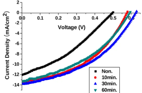
As shown in Figure 1, both open circuit voltage (VOC) and current density (JSC) were increased as the
annealing time increased for the gravure printed organic layers. VOC was improved by more than 20%
and ISC was improved by about 20%.
Figure 2 shows the power conversion efficiency as function of annealing time. Maximum power conversion efficiency of 3.6% was achieved with 30min annealing time. This result shows that device made from gravure printing is sensitive to annealing temperature. Molecular structure change with annealing temperature will be investigated further
Effect of Thermal Annealing of Gravure Printed Polymer
Solar Cells
Jiyeon Lee
1, Jungwoo Kim
2, Hyungsub Kim
2, Sung Min Cho
1and Heeyeop Chae
1*
1
School of Chemical Engineering, Sungkyunkwan University
2
School of Advanced Materials Science and Engineering, Sungkyunkwan University Suwon, 440-746, Korea
Tel.:82-31-290-7342, E-mail: [email protected]
P2-103 / J. Lee
• IMID 2009 DIGEST
Fig. 1. Current and voltage characteristics of polymer solar cells in this.
Fig. 2. Power conversion efficiency as function of annealing time.
As shown in Figure 3, current density was increased as the chloroform ratio of solvent increased for the gravure printed organic layers.
Fig. 3. Current and voltage characteristics of polymer solar cells by solvent ratio.
Figure 4 show the power conversion efficiency by the chloroform ratio of solvent. Maximum power conversion efficiency of 3.1% was achieved with chloroform ratio of 50%.
Fig. 4. Power conversion efficiency as function of solvent ratio.
4. Summary
We fabricated polymer solar cells based on P3HT:PCBM by changing the annealing time and solvent ratio for gravure printed organic layer. The best annealing time for device is postproduction treatment at 150 ℃ for 30min. The best solvent ratio is chloroform ratio of 50%.
Acknowledgement
This work was carried out with the support of the Korea Energy Management Corporation (Project No. 2007-E-CM11-P-07) and the Basic Research Program of the Korea Science & Engineering Foundation (Grand No. R01-2006-000-10140-0).
5. References
1. G. Li, V. Shrotriya, Y. Yao, and Y. Yang, J. Appl.
Phys., 98, 043704 (2005).
2. A. C. Mayer, M. T. Lloyd, D. J. Herman, Appl.
Phys. Lett., 85, 6272 (2004). 0.0 0.1 0.2 0.3 0.4 0.5 0.6 -14 -12 -10 -8 -6 -4 -2 0 2 Non. 10min. 30min. 60min. Cu rr en t D e n s it y ( mA /c m 2) Voltage (V)
Non 10min. 30min. 60min.
1.5 2.0 2.5 3.0 3.5 4.0 PC E ( % ) Time (min.) 0.0 0.1 0.2 0.3 0.4 0.5 0.6 -16 -14 -12 -10 -8 -6 -4 -2 0 2 DCB DCB:CF=9:1 DCB:CF=7:3 DCB:CF=5:5 C u rr e nt D e ns it y ( mA /c m 2) Voltage (V) DCB 9:1 7:3 5:5 1.5 2.0 2.5 3.0 3.5 PC E (% ) Solvent ratio (DCB:CF)