Regular Paper 681 J. Korean Inst. Electr. Electron. Mater. Eng.
Vol. 29, No. 11, pp. 681-684 November 2016 DOI: http://dx.doi.org/10.4313/JKEM.2016.29.11.681 ISSN 1226-7945 (Print), 2288-3258 (Online)
다양한 게이트 구조에 따른 IGBT 소자의 전기적 특성 비교 분석 연구
강이구a
극동대학교 태양광공학과
A Study Comparison and Analysis of Electrical Characteristics of IGBTs with Variety Gate Structures
Ey Goo Kang
aDepartment of Photovoltaic Engineering, Far East University, Eumseong 27601, Korea
(Received August 7, 2016; Revised September 24, 2016; Accepted October 5, 2016)
Abstract: This research was carried out experiments of variety IGBTs for industrial inverter and electric vehicle.
The devices for this paper were planar gate IGBT, trench gate IGBT and dual gate IGBT and we designed using same design and process parameters. As a result of experiments, the electrical characteristics of planar gate IGBT were 1,459 V of breakdown voltage, 4.04 V of threshold voltage and 4.7 V of on-state voltage drop. And the electrical characteristics of trench gate IGBT were 1,473 V of breakdown voltage, 4.11 V of threshold voltage and 3.17 V of on-state voltage drop. Lastly, the electrical characteristics of dual gate IGBT were 1,467 V of breakdown voltage, 4.14 V of threshold voltage and 3.08V of on-state voltage drop. We almost knew that the trench gate IGBT was superior to dual gate IGBT in terms of breakdown voltage. On the other hand, the dual gate IGBT was better than the trench gate IGBT in terms of on state voltage drop.
Keywords: Planar gate, Trench gate, Dual gate, High breakdown voltage, On state voltage drop
1. 서 론
1)IGBT (insulated gate bipolar transistor) 소자는 전류전도 능력이 뛰어난 소자이며, 큰 전력을 처리하기 위해 설계된 스위칭 디바이스로서 전원 공급 장치, 변 환기, 태양광 인버터, 가전제품 등에 널리 사용되고 있 다 [1,2]. 이러한 IGBT는 파워 반도체 소자인 만큼 항
a. Corresponding author; [email protected] Copyright ©2016 KIEEME. All rights reserved.
This is an Open-Access article distributed under the terms of the Creative Commons Attribution Non-Commercial License (http://creativecommons.org/licenses/by-nc/3.0) which permits unrestricted non-commercial use, distribution, and reproduction in any medium, provided the original work is properly cited.
복 전압과 온-상태 전압 강하, 스위칭 속도, 신뢰성의
이상적인 파워 반도체 소자의 요구사항을 목표로 하고
있다. 일반적으로 드리프트 영역의 농도를 낮추게 되면
항복 전압은 증가하지만 온 저항과 같은 기타 특성들
이 감소하게 되므로 설계의 최적화 및 구조 변경을 통
해 항복전압특성과 온-상태 전압 강하 특성을 개선 시
켜야 한다. 이렇듯 IGBT 소자의 효율을 높이기 위해
트레이드-오프 관계를 최적화하고자 여러 가지 구조들
이 나오고 있다. IGBT는 보편적으로 600 V∼1,700 V
급을 사용하는 스위칭 산업 분야 중 신재생 에너지용
인버터 분야, SMPS, 전기 자동차의 배터리 전원 장치
등 다양한 산업에서 필수적인 부품으로 사용되고 있다
682 J. Korean Inst. Electr. Electron. Mater. Eng., Vol. 29, No. 11, pp. 681-684, November 2016: E.-G. Kang
[3,5]. 또한 초고압 IGBT 분야에서는 송전 부분에서 전 력 변환 스위칭 및 고속 전철 전동장치 등에서 활용되 고 있다.
본 논문에서는 다양한 게이트 구조를 갖는 IGBT 소 자들에 대해 최적 설계 방안 및 전기적인 특성을 비교 하고자 플래너 게이트, 트렌치 게이트 및 듀얼 게이트 구조를 제안한 다음, T-CAD 툴을 이용하여 최적의 설 계 및 공정 변수를 도출하였다. 그리고 해당 소자들의 전기적인 특성을 비교 분석하고자 하였다.
2. 실험 방법
실험은 소자 및 공정 시뮬레이터인 T-CAD를 사용 하여 실험을 진행하였으며, 본 실험을 통해 각 소자들 의의 핵심 전기적인 특성에 영향을 주는 게이트 길이 와 JFET의 농도를 조절하여 특성을 비교분석 하였다.
또한 p-base 농도 조절을 통하여 전기적 특성 중 하 나인 온-상태 전압강하 특성을 비교하였다.
이러한 설계 및 공정 변수의 변화를 통한 플래너 게 이트, 트렌치 게이트 및 듀얼 게이트 IGBT의 전기적 특성을 비교 분석하였다.
2.1 플래너 게이트 IGBT 설계 및 실험
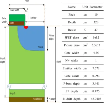
Name Unit Parameter
Pitch ㎛ 10
Depth ㎛ 320
Resist Ω 47
JFET dose cm2 1e12 P-base dose cm2 6.3e13
Gate width ㎛ 4.25
N+ width ㎛ 1
Emitter width ㎛ 7.571 Gate oxide ㎛ 0.093 P-bass depth ㎛ 3.441 P+ depth ㎛ 0.475 N-drift depth ㎛ 42.9402
Fig. 1. Structure of planer gate type IGBT and the parameters of design and process.
Fig. 2. Breakdown voltage characteristics of planar gate IGBT according to epi resistivity.
Fig. 3. On-state voltage drop and threshold voltage characteristics of planar gate IGBT according to p-base dose.
플래너 게이트 IGBT를 설계하기 위해 기본적인 파라 미터로 웨이퍼의 두께는 320 ㎛ 셀 피치는 10 ㎛로 고 정하고 실험을 진행하였다. 항복전압을 1,200 V로 선 택을 하였지만 마진율 20%를 고려한 1,450 V로 선택 하였으며 1,450 V에 최대한 가까운 지점을 찾기 위해 에피 비저항을 41 Ω∼49 Ω으로 변화시키면서 시뮬레 이션을 실행하여 1,450 V에 최대한 가까운 1,459.08 V 를 얻을 수 있었다.
20%의 마진을 고려한 항복전압을 설계한 후 그 값
을 얻을 수 있는 에피의 비저항을 47 Ω으로 고정하고
p-base의 농도를 6.1×10
13㎠∼6.9×10
13㎠으로 조절한
후 문턱전압 4 V를 얻을 수 있는 농도에서 Vce-sat의
값을 도출하고자 하였다. 이러한 실험을 수행하여 플래
나 게이트 IGBT의 문턱전압은 4.04 V 및 온-상태 전
압강하는 4.69 V를 얻을 수 있었다.
전기전자재료학회논문지, 제29권 제11호 pp. 681-684, 2016년 11월: 강이구 683
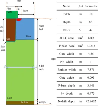
2.2 트렌치 게이트 IGBT 설계 및 실험
본 절에서는 현재 스위치소자로 가장 많이 활용되고 있는 트렌치 게이트 IGBT 구조는 플래나 게이트 IGBT 구조와 같은 웨이퍼의 두께 320 ㎛, 셀 피치 10 ㎛로 크기를 지정하였다. 항복전압인 BV를 1,450 V에 가까 운 지점을 찾기 위해 플래나 게이트 구조에서 수행했 던 실험과 동일한 방법으로 에피 비저항을 41 Ω∼49 Ω까지 변화시키면서 실험을 실행하여 동일한 에피 비 저항을 47 Ω로 선정 시 1,450 V에 가까운 1,475.12 V 를 확인하였다. 이전에 수행했던 플래나 게이트 IGBT 의 항복전압보다 15 V 이상의 높은 항복전압을 얻을 수 있었다.
그림 4에서는 트렌치 게이트 IGBT 구조와 설계 및 공정파라미터를 보여주고 있다. 그림 5는 에피 저항에 따른 항복전압을 보여주고 있으며, 그림에서 보여주는 것처럼 에피 저항 47 Ω에서 1,475 V의 항복전압을 얻을 수 있었다. 트렌치 게이트 IGBT의 온-상태 전압 을 얻기 위해서 에피 비저항을 47 Ω으로 고정하고 p-base의 dose를 1×10
13㎠∼4.5×10
13㎠으로 조절하 여 4 V의 문턱전압을 예측하였으며, 이 때 온-상태 전 압강하의 값을 도출하고자 하였다. 그림 6에서는 실험 을 하여 최종적으로 얻은 온-상태 전압강하특성을 보 여주고 있다.
Name Unit Parameter
Pitch ㎛ 10
Depth ㎛ 320
Resist Ω 47
JFET dose cm2 1e12 P-base dose cm2 6.3e13 Gate width ㎛ 4.25
N+ width ㎛ 1
Emitter width ㎛ 7.571 Gate oxide ㎛ 0.093 P-bass depth ㎛ 3.441 P+ depth ㎛ 0.475 N-drift depth ㎛ 42.9402
Fig. 4. Structure and design parameters of trench gate type IGBT.
Fig. 5. Breakdown voltage characteristics of planar gate IGBT according to epi resistivity.
Fig. 6. On-state voltage drop and threshold voltage characteristics of planar gate IGBT according to p-base dose.
그림 6에서 볼 수 있는 것처럼, 문턱전압이 4.11 V 그리고 온-상태 전압강하 값이 3.18 V을 가져 올 수 있는 p-base의 농도는 2×10
13㎠로 알 수 있었다. 또 한 온-상태 전압강하 특성 또한 플래너 게이트 IGBT 보다 우수한 것을 알 수 있었으며, 그것은 전류가 흐 르는 채널 저항이 트렌치 구조에 의해서 줄어들었기 때문임을 알 수 있다.
2.3 듀얼 게이트 IGBT 설계 및 실험
본 논문에서는 또한, 앞서 서술하였던 플래나 게이
트 및 트렌치 게이트와 같은 설계 및 공정변수를 이용
하여 듀얼게이트 소자를 설계하여 실험을 진행하였으
며, 같은 문턱전압 조건과 p-base 농도를 조절하여 항
복전압과 온-상태 전압 강하 값을 도출하고자 하였다.
684 J. Korean Inst. Electr. Electron. Mater. Eng., Vol. 29, No. 11, pp. 681-684, November 2016: E.-G. Kang
그림 7은 듀얼 게이트 구조의 IGBT 소자를 보여주 고 있으며, 실험을 진행한 결과 트렌치 게이트 IGBT 소자보다 약간 낮은 1,469 V의 항복전압을 얻은 반면, 온-상태 전하 강하 값은 트렌치 게이트 IGBT 구조보 다 효율적인 3.08 V의 값을 얻을 수 있었다.
Fig. 7. Structure of dual gate type IGBT.
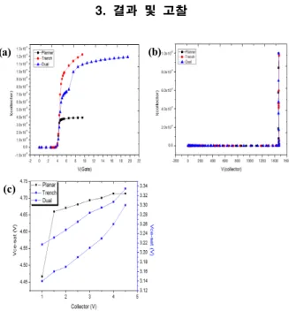
3. 결과 및 고찰
(a) (b)
(c)
Fig. 8. The electrical characteristics of planar gate type IGBT, trench gate type IGBT and dual gate type IGBT (a) Vth, (b) BV, and (c) Vce-sat.
앞 절에서 진행한 3개의 소자에 대해서 비교 분석한 결과를 표 1에서 보여주고 있으며, 그림 8에서는 해당 소자들의 전기적인 특성인 항복전압, 문턱전압 및 온- 상태 전압 강하 특성을 보여주고 있다.
Table 1. The electrical characteristics of planar gate type IGBT, trench gate type IGBT and dual gate type IGBT.
IGBT Planar gate Trench gate Dual gate
BV 1,459.08 1,473.12 1,467.04
Vth 4.04 4.11 4.14
Vce-sat 4.694 3.17 3.084
4. 결 론
본 논문에서는 산업용 인버터, 가전 및 전기자동차 용에 가장 많이 활용되고 있는 1,200 V급의 다양한 I GBT소자들에서 대해서 전기적 특성을 비교 분석하였 다. 본 연구에서 진행된 소자는 플래나 게이트 구조의 IGBT, 트렌치 게이트 구조의 IGBT 및 플래나와 트렌 치의 구조를 혼합한 듀얼게이트 구조의 IGBT 소자이 며, 각각의 소자들에 대해서 같은 설계 및 공정변수를 이용하여 설계 및 실험을 진행하였다. 실험을 진행한 결과 항복전압은 트렌치 게이트 IGBT가 1,473 V의 우 수한 결과를 가져올 수 있었으며, 온-상태 전압 강하 값은 듀얼게이트 IGBT 구조가 상대적으로 3.084 V의 낮은 값을 얻을 수 있었다. 또한 듀얼게이트 IGBT 구 조의 항복전압도 트렌치 게이트보다 낮지만 비교적 안 정적인 값을 도출할 수 있었다. 최근의 가장 이슈가 되는 전력소모적인 측면에서는 듀얼 게이트 IGBT가 상 당히 효과적인 것을 알 수 있었다.
REFERENCES
[1] E. G. Kang, D. S. Oh, D. W. Kim, D. J. Kim, and M. Y.
Sung, J. Korean Inst. Electr. Electron. Mater. Eng., 15, 758 (2002).
[2] J. I. Lee, S. M. Yang, Y. S. Bae, and M. Y. Sung, J.
Korean Inst. Electr. Electron. Mater. Eng., 23, 190 (2010).
[3] T. Laska, M. Munzer, F. Pfirsch, C. Schaeffer, and T.
Schmidt, ISPSD Proceedings, 355 (2000). [DOI: http://
dx.doi.org/10.1109/ispsd.2000.856842]
[4] B. S. Ahn, H. S. Chung, E. S. Jung, S. J. Kim, and E.
G. Kang, J. Korean Inst. Electr. Electron. Mater. Eng., 25, 187 (2012).
[5] J. S. Lee, E. G. Kang, and M. Y. Sung, Microelectronics Journal, 39, 57 (2008). [DOI: http://dx.doi.org/10.1016/j.
mejo.2007.10.023]