364 J. Sensor Sci. & Tech. Vol. 24, No. 6, 2015 Journal of Sensor Science and Technology
Vol. 24, No. 6 (2015) pp. 364-367 http://dx.doi.org/10.5369/JSST.2015.24.6.364 pISSN 1225-5475/eISSN 2093-7563
Optical and Electronic Properties of SnO 2 Thin Films Fabricated Using the SILAR Method
Joohee Jang
1,2, Haena Yim
1, Yoon-Ho Cho
1, Dong-Heon Kang
2, and Ji-Won Choi
1,+Abstract
Tin oxide thin films were fabricated on glass substrates by the successive ionic layer adsorption and reaction (SILAR) method at room temperature and ambient pressure. Before measuring their properties, all samples were annealed at 500
oC for 2 h in air. Film thickness increased with the number of cycles; X-ray diffraction patterns for the annealed SnO
2thin films indicated a SnO
2single phase. Thickness of the SnO
2films increased from 12 to 50 nm as the number of cycles increased from 20 to 60. Although the optical transmittance decreased with thickness, 50 nm SnO
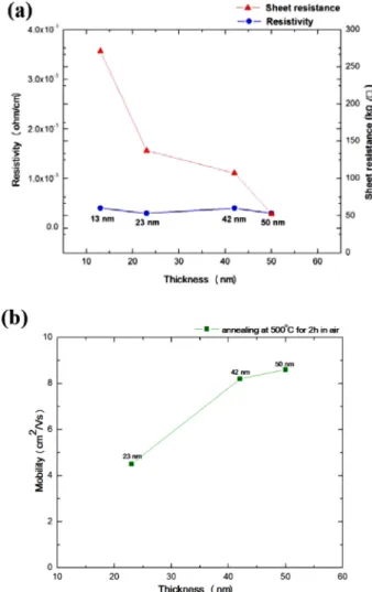
2thin films exhibited a high value of more than 85%. Regarding electronic properties, sheet resistance of the films decreased as thickness increased; however, the measured resistivity of the thin film was nearly constant with thickness (3 ×10
-4ohm/cm). From Hall measurements, the 50 nm thickness SnO
2thin film had the highest mobility of the samples (8.6 cm
2/(V·s)). In conclusion, optical and electronic properties of SnO
2thin films could be controlled by adjusting the number of SILAR cycles.
Keywords: SnO
2, Oxide semiconductors, SILAR method
1. INTRODUCTION
In recent years, transparent oxide semiconductors (TOS) have received significant attention for application in a wide range of electronic devices requiring transparency, such as light emitting diodes, solar cells, optical sensors, CMOSs and displays [1]. One such transparent oxide semiconductor material is tin oxide (SnO
2), which has high optical transmittance in the visible range and low electrical resistance [2-4]. SnO
2is an n-type semiconductor that forms as a result of an excess of electrons produced by ionization of oxygen vacancies, and interstitial tin atoms that are generated during the crystal growth process. In addition, SnO
2thin films are mechanically strong and thermally stable in oxidizing environments at high temperatures, and chemically stable in both acidic and basic solutions. However, compared to other TOS materials, SnO
2films exhibit poor performance in some areas,
such as having low values for mobility and for on-off ratio. The optical and electronic properties of SnO
2films can be improved by doping. The upper limit on the electron density, which determines mobility, is set by the solubility of the dopants.
However, if the concentration of dopants introduced exceeds the maximum solubility, the excess can form clusters in the lattice, accompanied by a loss of crystallinity. An increased sheet resistance then occurs as a result of atomic disorder and impurity scattering, which reduces mobility of the electrical carriers [5].
However, the presence of impurities at grain boundaries can reduce the barriers between crystallites and may consequently increase the mobility and decrease the sheet resistance [6].
Properties of SnO
2films impurity-doped with group III, V, VI, and VII elements [6] such as In, F [7], Te, Sb, Cl [8], Al, and Br [8]
have been studied. SnO
2can be either an n-type or p-type semiconductor, determined easily by dopant selection. Before considering such modification of SnO
2films, uniform SnO
2thin films should be investigated as preceding researches. Many researches groups have studied fabrication of SnO
2thin films using various ways such as vacuum evaporation, sputtering [9], CVD, MOCVD, and spray pyrolysis [8]. A chemical method for the deposition of a thin film is the successive ionic layer adsorption and reaction (SILAR) method, which has a number of advantages, including a simple procedure. The SILAR method is known as modified version of chemical bath deposition method by which thin films of compound semiconductors can be
1
Center for Electronic Materials, Korea Institute of Science and Technology, Seoul 136-791, Korea
2
Department of Electronic Materials Engineering, University of Suwon, Suwon 445-743, Korea
+