Regular Paper 18 J. KIEEME
Vol. 27, No. 1, pp. 18-21 January 2014
DOI: http://dx.doi.org/10.4313/JKEM.2014.27.1.18
Pulsed Laser Deposition 방법으로 증착된 ZnSnO
3압전 박막의 성장과 특성 평가
박병주1, 윤순길1,a
1 충남대학교 재료공학과
Fabrication and Properties of ZnSnO
3Piezoelectric Films Deposited by a Pulsed Laser Deposition
Byeong-Ju Park1 and Soon-Gil Yoon1,a
1 Department of Materials Engineering, Chungnam National University, Daejeon 305-764, Korea
(Received October 11, 2013; Revised November 19, 2013; Accepted November 21, 2013)
Abstract: Because the Pb-based piezoelectric materials showed problems such as an environmental pollution. lead-free ZnSnO3 materials were studied in the present study. The ZnSnO3 thin films were deposited at 640℃ on Pt/Ti/SiO2 substrate by pulsed laser deposition (PLD) and were annealed for 5 min at 750℃ using rapid thermal annealing (RTA) in nitrogen atmosphere. Samples annealed at 750℃ showed a smooth morphology and an improvement of the dielectric and leakage properties, as compared with as-grown samples. However, electrical properties of the ZnSnO3 thin films obtained in the present study should be improved for piezoelectric applications.
Keywords: ZnSnO3 thin film, Pulsed laser deposition, Rapid thermal annealing
1. 서 론1)
최근의 기억소자 집적기술은 고속화와 더불어 대용 량화가 활발히 연구되고 있다. 이 중 커패시터는 전 자부품에 3차원적으로 적층되어 부품의 전체 체적이 증가하게 되고 커패시터를 저항에 연결할 때에 연결 부분에 의한 손실이 증가되는 단점을 보인다. 이에 따라 이들을 박막화함으로써 체적을 줄이고 곧바로 PCB (printed circuit board)에 임베딩 하여 여러 가 지 손실을 줄이는 연구가 진행되고 있으며 더불어 충
a. Corresponding author; [email protected] Copyright ©2014 KIEEME. All rights reserved.
This is an Open-Access article distributed under the terms of the Creative Commons Attribution Non-Commercial License (http://creativecommons.org/licenses/by-nc/3.0) which permits unrestricted non-commercial use, distribution, and reproduction in any medium, provided the original work is properly cited.
분한 정전용량을 보유하기 위한 방안으로 유전상수가 큰 재료의 개발이 진행되고 있다 [1,2]. 유전상수가 큰 세라믹 재료의 대표적 물질인 PZT (Pb(Zr,Ti)O3)는 많 은 연구와 응용이 이루어지고 있지만 산화납의 독성, 환경유해성으로 인해 lead-free계 재료의 개발이 전 세 계적으로 심각하게 대두되고 있다. 이 가운데 2008년 Inaguma그룹에서 lead-free한 신물질 ZnSnO3의 구조적 특성을 보고한데 이어 Shin 그룹에서 ZnSnO3의 강유전 체 특성 연구를 시작으로 열역학적 분석, 화학적 결합, 유전특성 예측 등 다양한 연구가 진행되고 있다 [3-7].
본 연구에서는 PLD (pulsed laser deposition)법을 이용하여 Pt/Ti/SiO2 기판에 ZnSnO3를 증착하고 급 속열처리 (rapid thermal annealing, RTA)와 상부전 극 열처리를 통하여 아직 보고되지 않은 ZnSnO3 박 막의 누설전류밀도와 정전용량을 평가하였다.
전기전자재료학회논문지, 제27권 제1호 pp. 18-21, 2014년 1월: 박병주 등 19
2. 실험 방법 2.1 ZnSnO3 박막의 제조
ZnSnO3 박막은 PLD법을 이용하여 증착하였다.
표 1은 PLD법을 이용한 ZnSnO3 박막의 증착 조건 을 나타낸다. ZnSnO3 박막은 기판 온도 600, 640℃에 서 초 당 4 shots (4 Hz), 1.3 J/cm2의 레이저 밀도가 조사되도록 하였다. ZnSnO3 박막의 증착은 타겟과 기 판과의 거리를 6 cm로 유지하면서 200 mTorr, O2 50 sccm의 분위기에서 Pt(200 nm)/Ti(3 nm)/SiO2 기판 에 증착하였다. 제조된 박막은 주사전자현미경 (scanning electron microsope, SEM)을 통해 단면과 표면을, X-ray 회절 분석 (X-ray diffraction pattern, XRD)을 통해 결정 화를, 에너지 분광 (energy dispersive spectrometer, EDS)을 통하여 완성된 ZnSnO3 박막의 조성을 확인하였다.
Table 1. Deposition conditions of ZnSnO3 thin films by PLD.
Parameters ZnSnO3 thin film
Target ZnSnO3
Laser power density 1.3 J/cm2
Repetition rate 4 Hz
Substrate temperature 640℃
Working pressure 200 mTorr
O2 flow rate 50 sccm
2.2 ZnSnO3 박막의 급속 열처리
본 연구에서는 PLD법을 이용하여 ZnSnO3 박막을 증착할 때 진공 상태에서 640℃ 이상 승온시킬 수 없 어 ZnSnO3 박막의 결정화도 증가를 위해서 급속 열 처리를 수행하였다. 열처리 시 O2 분위기에서는 하부 전극으로 이용되는 Pt가 O2와 반응하여 전극으로서의 기능을 상실하기 때문에 15 mTorr까지 진공을 만든 후, 상온에서 N2 100 sccm으로 상압에 도달시킨 후 N2 분위기에서 750℃에서 5분간 진행되었다.
급속 열처리 후 ZnSnO3/Pt/Ti/SiO2 시편에 Pt상부 전극을 DC-sputtering법으로 증착했다. 상부전극이
Table 2. Rapid thermal annealing conditions of ZnSnO3
thin films.
Parameters RTA
Substrate temperature 750℃
Working pressure 760 Torr
N2 flow rate 100 sccm
Annealing time 5 min
증착된 시편은 상부전극과 박막의 계면 사이에 공간 전하 (space charge)를 제거하기 위하여 O2 (100 sccm)으로 상압에 도달시킨 후 급속 열처리를 이용해 400℃에서 30분 동안 상부전극 열처리를 진행하였다.
완성된 ZnSnO3 박막은 HP4156B를 통해 누설전류를, HP4194A를 통해 정전용량을 측정하였다.
3. 결과 및 고찰
Fig. 1. XRD patterns of the ZnSnO3 films grown on Pt/Ti/SiO2 at (a) 600, (b) 640℃, and (c) annealed at 750℃
after deposition at 640℃.
그림 1은 600, 640℃에서 증착된 ZnSnO3 박막과 640℃에서 증착된 박막을 750℃에서 열처리된 ZnSnO3
박막의 X-ray 회절 패턴을 보여주고 있다. 기판 온도 600℃에서 증착된 (a)에서는 ZnSnO3 박막의 결정화가 거의 이루어지지 않았지만 기판 온도 (b) 640℃에서 부 터 ZnSnO3 박막이 결정화되는 것을 확인하였다.
20 J. KIEEME, Vol. 27, No. 1, pp. 18-21, January 2014: B.-J. Park et al.
Fig. 2. SEM cross-sectional ((a) and (c)) and surface images ((b) and (d)) of ZnSnO3 films as-grown on Pt/Ti/SiO2 at 640℃ and annealed at 750℃, respectively.
(b)
Fig. 3. (a) SEM surface image of as-grown ZnSnO3
films and (b) EDS spectrum of the ZnSnO3 films.
그리고 (c) 750℃에서 급속 열처리된 ZnSnO3 박막 은 열처리로 인한 상분리 없이 결정화가 이루어진 것 을 확인할 수 있다. PLD법으로 증착된 ZnSnO3 박막 의 SEM 단면과 표면 이미지를 그림 2에 나타내었다.
(a), (b)를 통해 기판 온도 640℃에서 Pt/Ti/SiO2 위에 증착된 ZnSnO3 박막의 성장 상태를 확인할 수 있었 고 (c), (d) 750℃ 열처리에서도 열처리 전과 동일한 300 nm 두께의 ZnSnO3 박막의 상태를 확인할 수 있었지만
Table 3. Elemental Composition of ZnSnO3 films.
Elements Wt% At%
O K 10.05 29.82
Zn L 14.09 10.23
Sn L 29.07 11.63
Pt L 34.36 8.36
Fig. 4. Relationship between leakage current density and applied voltage for as-grown samples and annealed at 750℃.
하부전극으로 쓰인 Pt가 640℃로 승온되는 동안 입계 가 성장하여 표면 거칠기가 커져 ZnSnO3 박막의 표 면 역시 굉장히 거친 것을 알 수 있다. 이런 거친 표 면은 하부전극-박막, 박막-상부전극간에 계면 결함을 발생시켜 전자 소자로서의 기능을 크게 감소시키는 원인이 된다.
그림 3(a)는 기판 온도 640℃에서 동일한 300 nm 두께로 증착되어진 ZnSnO3 박막의 표면 이미지이다.
증착된 ZnSnO3 박막은 (b) EDS 분석을 통하여 성분 분석이 이루어졌다.
표 3은 Zn와 Sn의 조성이 약 1:1로 유사하게 이루 어지고 있음을 보여주고 있다.
그림 4(a)는 640℃에서 증착된 ZnSnO3 박막의 누설 전류밀도 특성을 나타낸 것이다. 640℃에서 증착된 ZnSnO3 박막의 누설전류밀도값이 높은 것을 확인할 수 있는데 이는 하부전극으로 사용된 Pt가 640℃에서 결정립 조대화로 인해 표면 거칠기가 크게 증가한 상
전기전자재료학회논문지, 제27권 제1호 pp. 18-21, 2014년 1월: 박병주 등 21
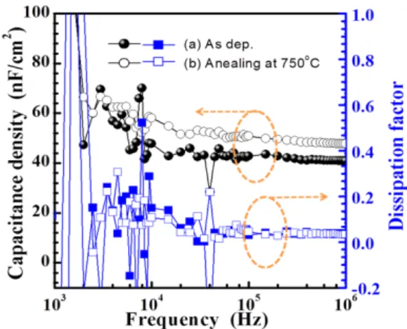
Fig. 5. Capacitance and dissipation factor as a function of frequency of the samples as-grown and annealed at 750℃.
태가 되고, 그 위에 ZnSnO3 박막을 증착하여 생긴 하 부전극과 박막 사이에 계면 결함이 주원인으로 사료 된다.
그림 4(b)는 640℃에서 증착된 ZnSnO3 박막을 750℃
에서 5분간 열처리를 거친 시료의 누설전류 값을 나타 낸다. 인가된 전압이 0 V에서 2 V까지 변할 때 열처리 전에 보다 10-2 A/cm2 정도의 누설전류 감소를 확인할 수 있다.
그림 5(a)는 640℃에서 증착된 ZnSnO3 박막을, (b) 는 750℃에서 5분간 열처리를 거친 박막의 정전용량 특성을 나타낸 것이다. 104 Hz 이하에서는 정전용량 특성이 불안정한 것을 볼 수 있는데 이는 누설전류 특성과 마찬가지로 전극과 박막 사이에 계면 결함이 주원인으로 판단된다. (a) 640℃에서 증착된 ZnSnO3
박막은 100 kHz에서 C= 42.8 nF/cm2, D= 0.03, εr= 14의 값을 나타내었고, (b) 750℃에서 5분간 열처리를 거친 박막은 100 kHz에서 C= 51.85 nF/cm2, D= 0.02, εr= 18로서 열처리 전보다 향상된 특성을 나타내었다.
4. 결 론
본 연구에서는 PLD법을 이용하여 기판 온도 640℃
에서 Pt/Ti/SiO2 위에 증착된 ZnSnO3 박막과 750℃에서
열처리된 박막의 전기적 특성을 비교하였다.
상부전극 열처리는 두 개의 시료 모두 400℃에서 30분간 동일하게 진행되었다. ZnSnO3 박막은 열처리 후에도 박막 성분의 혼재 없이 동일한 성분, 결정화 도를 가지고 있는 것을 확인하였다. 750℃에서 열처리된 ZnSnO3 박막은 열처리 전보다 부드러운 표면을 가짐으 로 인해 2 V에서 10-2 A/cm2 정도의 누설전류 감소를 보였고 정전용량 역시 향상된 값을 나타내었다. 하지 만 상부, 하부전극과 ZnSnO3 박막의 계면 상태가 고 르지 못해 높은 누설전류밀도값과 낮은 정전용량값을 나타내었다. 이는 증착 과정 중에 하부전극으로 사용 된 Pt의 입계가 고온에서 성장하여 큰 표면 거칠기를 나타내었기 때문이다. 추후 계면 결함을 없애기 위해 고온에서 안정한 세라믹 재료 전극을 이용한 실험이 요구된다.
REFERENCES
[1] H. A. Song, B. J. Park, and S. G. Yoon, J.
KIEEME, 25, 5 (2012).
[2] S. I. Swartz and V. E. Wood, Condensed Mat.
News, 1, 5 (1992).
[3] Y. Inaguma, M. Yoshida, and T. Katsumata, J. Am.
Chem. Soc., 130, 21 (2008).
[4] J. Y. Son, G. H. Lee. M. H. Jo, H. G. Kim, H. M.
Jang, and Y. H. Shin, J. Am. Chem. Soc., 131, 24 (2009).
[5] H. Wang, H. Huang, and B. Wang, Solid State Commun., 149, 1849 (2009).
[6] M. Nakayama, M. Nogami, M. Yoshida, T.
Katsumata, and Y. Inaguma, Adv. Mater., 22, 2579 (2010).
[7] J. Zhang, K. L. Yao, Z. L. Liu, G. Y. Gao, Z. Y.
Sun, and S. W. Fan, PCCP, 12, 9197 (2010).