- 2269 -
Shift register를 이용한 Zigbee 모듈의 PN 코드 생성기 설계
정 민교* , 김 인수*, 민 형복*, 최 재덕**
성균관대학교 정보통신공학부*, 대림대학 컴퓨터정보계열**
Design PN Code generator of Zigbee module using Shift Register
Min Kyo Jung*, Insoo Kim*, Hyoung Bok Min*, Jae-Duck Choi**
School of Information&Communication Engineering, Sungkyunkwan University*
Division of Computer Science and Information, Daelim College**
Abstract - Zigbee that is the wireless personal area networks communication technology for low power consumption is low-cost, low-power consumption, and small size and program code. From the present paper symbol and chip sequence of existing Zigbee module undergarment PN code generators which are a 1:1 mapping method it uses shift register and it plans the method which it proposes. The experimental result used Xilinx ISE and it measured synthesis and timing and power.
1. 서 론
저전력 무선 근거리 표준 통신 기술인 Zigbee는 가격이 저렴하고, 전 력소모가 매우 적고, 크기와 프로그램이 작다. 근거리에서 속도가 크게 빠르지 않고, 네트워크 사용 빈도가 드문 경우 가장 적합하다. 그러나 기존의 Zigbee 모듈 내의 PN 코드 생성기는 Symbol에 따른 Chip Sequence를 1:1 mapping하여 출력하는 방식으로 ROM을 사용하여 size 가 크다.. 본 논문에서는 기존의 Symbol와 Chip sequence의 1:1 mapping 방식이 아닌 Shift register를 이용한 Symbol에 따른 Chip Sequence를 출력하는 방법을 제안한다. Zigbee 모듈내에서 ROM을 제 거함으로써 동일한 전력과 속도임에도 불구하고 chip size를 줄일 수 있 다.
2. 본 론
2.1 IEEE 802.15.4 변조회로
IEEE 802.15.4 변조회로는 물리계층에서 PPDU를 입력받아 8bit 단위로 끊고 다시 4bit씩 끊는다. 그 Niddle(4bit)을 PN부호 열에 대입하여 Bit-to-Symbol의 과정을 거쳐서 심볼값을 얻고, 해당 심볼에 맞는 Chip을 얻는다. 그 chip을 I/Q 상으로 나눠 이 를O-QPSK변조 한 후 전송하게 된다.[2],[3]
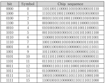
<그림 1> IEEE 802.15.4 변조회로 2.2 Symbol과 Chip Sequence의 mapping
<표 1> Symbol과 Chip sequence mapping
bit Symbol Chip sequence
0000 0 11011001110000110101001000101110 1000 1 11101101100111000011010100100010 0100 2 00101110110110011100001101010010 1100 3 00100010111011011001110000110101 0010 4 01010010001011101101100111000011 1010 5 00110101001000101110110110011100 0110 6 11000011010100100010111011011001 1110 7 10011100001101010010001011101101 0001 8 10001100100101100000011101111011 1001 9 10111000110010010110000001110111 0101 10 01111011100011001001011000000111 1101 11 01110111101110001100100101100000 0011 12 00000111011110111000110010010110 1011 13 01100000011101111011100011001001 0111 14 10010110000001110111101110001100 1111 15 11001001011000000111011110111000
표 1에서 보여지듯, “Bit-to-symbol"에서 PPDU에서 받은 4bit를 LSB 부터 먼저 받아들여 이를 해당되는 symbol로 mapping 하고
“Symbol-to-chip"에서 symbol에 해당되는 Chip sequence를 1:1로 mapping하여 출력한다.[2],[4]
2.3 제안하는 방법
표 1에서 볼 수 있듯이 Symbol 0에서 Symbol 7까지 해당되는 Chip sequence는 Symbol이 1씩 차이날 때마다 4bit씩 shift되는 bitpattern을 가지고, 마찬가지로 Symbol 8에서 Symbol 15까지 해당되는 Chip sequence는 Symbol이 1씩 차이날 때마다 4bit씩 shift되는 bitpattern을 가진다. 이를 바탕으로 Symbol 3과 Symbol 11의 Chip sequence를 기준 으로 입력되는 symbol과의 차이만큼 Chip sequence를 shift 함으로써 기존의 1:1 mapping 방식과 동일한 연산결과를 출력할 수 있다. symbol 15개 대한 Chip sequence를 모두 가지는 것이 아닌, 단지 Symbol 2개에 해당되는 Chip sequence만 가짐으로서 기존의 mapping 방식에 비해 불 필요한 ROM을 제거함으로써 size를 개선할 수 있다.
3. 실 험 결 과
본 논문에서 제안하는 구조의 검증을 위해, 기존의 mapping방 식과 제안하는 구조의 방식을 각각 VHDL code로 작성한 후 Xilinx ISE 10.1을 이용하여 Synthesis한 후 cell의 사용빈도를 측정하고, Xilinx Xpower Analysis를 이용하여 소모되는 전력을 측정하였다.[1]
2008년도 대한전기학회 하계학술대회 논문집 2008. 7. 16 - 18
- 2270 -
<그림 2> Shift register를 이용한 PN코드생성기 회로
보다 정확한 simulation을 위해 CPLD model을 제외하고, spartan2(xc2s200-5q-fg456), spartan3(xc3s200-5-vq100), spartan3E(xc3s1600E-5-fg400), virtex5(xc5blx50t-3-ff1136), virtexE(xcv600e-8-fg900)를 사용하였다.
<표 2> Advanced HDL Synthesis 결과
device mapping shift reg.
spartan2 xc2s200-5q-fg456
ROM(RAM) 1 0
flip-flop 32 32
etc 0 3
spartan3 xc3s200-5-vq100
ROM(RAM) 1 0
flip-flop 32 32
etc 0 3
spartan3E xc3s1600E-5-fg400
ROM(RAM) 1 0
flip-flop 32 32
etc 0 3
virtex5 xc5blx50t-3-ff1136
ROM(RAM) 1 0
flip-flop 32 32
etc 0 3
virtexE xcv600e-8-fg900
ROM(RAM) 1 0
flip-flop 32 32
etc 0 3
<표 3> timing 및 power simulation 결과
(input ≜minimum input arrival time before clock, output ≜ Maximum output required time after clock)
device mapping shift reg.
spartan2 xc2s200-5q-fg456
input 3.609ns 7.400ns ouput 10.481ns 7.999ns
power 25mW 25mW
spartan3 xc3s200-5-vq100
input 4.687ns 4.687ns ouput 6.216ns 6.216ns
power 41mW 41mW
spartan3E xc3s1600E-5-fg400
input 4.117ns 4.117ns ouput 4.040ns 4.040ns
power 207mW 203mW
virtex5 xc5blx50t-3-ff1136
input 2.124ns 2.124ns ouput 2.775ns 2.775ns
power 446mW 446mW
virtexE xcv600e-8-fg900
input 2.495ns 5.122ns ouput 7.316ns 5.783ns
power 303mW 303mW
4. 결 론
본 논문에서는 제안하는 구조인 Shift register를 이용하여 Zigbee module내의 Symbol-to-Chip의 size를 개선하였다.
기존의 Symbol과 Chip sequence의 mapping 방식은 모든 input에 대한 output값을 저장할 ROM을 포함하고 있었으나, 본 논문에서 제안한 Shift register를 이용한 PN코드 생성기는 같은 시간과 power에도 불구하고 ROM을 제거함으로써 chip의 size를 줄여 보다 집적화가 가능해진다.
[참 고 문 헌]
[1] Charles H. Roth, Jr., "Digital Systems Design Using VHDL", PWS Publishing Company, 1998.
[2] IEEE Std 802.15.4™-2003 Part 15.4: Wireless Medium Access Control (MAC) and Physical Layer (PHY) Specifications for Low-Rate Wireless Personal Area Networks (LR-WPANs)
[3] ZigBee Document 053474r06, Version 1.0 [4] Radiopulse MG2400-F48 Datasheet