1. INTRODUCTION
Global Positioning System (GPS) is a system that has been developed by the U.S. Department of Defense for military purposes. GPS has been actively used in the civilian sector since 2000, and it is currently used in various fields. A GPS receiver is vulnerable to jamming signals because it receives signals transmitted from satellites at about 20,000 km above the Earth and because all the signal characteristics (e.g., frequency, modulation method, and code) are open to the public (Kaplan & Hegarty 2006).
The recent GPS jamming from North Korea was a simple
ABSTRACT
Global Positioning System (GPS) is used in various fields such as communications systems, transportation systems, e-commerce, power plant systems, and up to various military weapons systems recently. However, GPS receiver is vulnerable to jamming signals as the GPS signals come from the satellites located at approximately 20,000 km above the earth. For this reason, various anti-jamming techniques have been developed for military application systems especially and it is also required for commercial application systems nowadays. In this paper, we proposed a dual-channel Global Navigation Satellite System (GNSS) RF ASIC for digital pre-correlation anti-jam technique. It not only covers all GNSS frequency bands, but is integrated low-gain/attenuation mode in low-noise amplifier (LNA) without influencing in/out matching and 14-bit analog- digital converter (ADC) to have a high dynamic range. With the aid of digital processing, jamming to signal ratio is improved to 77 dB from 42 dB with proposed receiver. RF ASIC for anti-jam is fabricated on a 0.18-μm complementary metal-oxide semiconductor (CMOS) technology and consumes 1.16 W with 2.1 V (low-dropout; LDO) power supply. And the performance is evaluated by a kind of test hardware using the designed RF ASIC.
Keywords: GNSS, anti-jamming, RF ASIC, CMOS, high dynamic-range receiver
type of jamming signal, but it is a strong threat since all the position and time information based on GPS could be disturbed (Hu & Wei 2009). Jamming signals could induce significant disturbance in the civilian fields based on GPS as well as jamming for the military weapon systems. Thus, preparation for this incident is needed. For the removal of jamming signals, various studies have been performed such as an antenna-based anti-jamming technique and a digital signal processing technique (Abimoussa & Landry 2000, Amin & Sun 2005). To apply a technique for the removal of jamming signals, satellite signals that are smaller than thermal noise and jamming signals that are relatively significantly large need to be converted into digital signals without distortion and sent to a jamming removal signal processing part. Therefore, to implement an anti-jamming function, the RF part of a Global Navigation Satellite System (GNSS) receiver needs to have low-noise characteristics as Received July 31, 2015 Revised Aug 19, 2015 Accepted Aug 25, 2015
†
Corresponding Author E-mail: [email protected]
Tel: +82-42-363-9283 Fax: +82-42-363-9001
well as wider dynamic range and linearity compared to an existing general GNSS receiver (Moulin et al. 1998). In this study, high-sensitivity/high-resolution RF ASIC with a wide dynamic range was designed and manufactured so that it could be used for the implementation of a jamming signal removal function, and an anti-jamming device based on digital signal processing that removes narrowband jamming signals in the frequency domain was implemented and the performance was verified.
2. DESIGN OF RF ASIC FOR AN ANTI- JAMMING GNSS RECEIVER
In a general GNSS receiver, the RF front-end appropriately amplifies and filters satellite signals received at a signal strength of about -130 dBm, converts them into digital signals using analog-digital converter (ADC) with effective number of bits (ENOB) of 1.5 ~ 2, and sends them to a digital signal processing part. For satellite signals, the change in the strength of received signals depending on the altitude of satellites is not large (less than 3 dB), and the quantization error can be reduced to less than 1 dB through an appropriate use of AGC. Thus, 2 bit (ENOB) ADC is sufficient for a general GNSS receiver (Parkinson & Spilker 1996). However, an anti- jamming GNSS receiver needs to quantize both satellite signals and jamming signals without distortion and send them to a digital signal processing part even when jamming signals that are more than 50 ~ 70 dB larger than satellite signals are introduced to the receiver along with satellite signals. Therefore, RF ASIC to be implemented should have a wide dynamic range of more than 50 dB and have high- resolution and low-noise characteristics. In general, an anti- jamming receiver uses 12 ~ 14 bit ADC.
2.1 Analysis of the Dynamic Range of RF ASIC
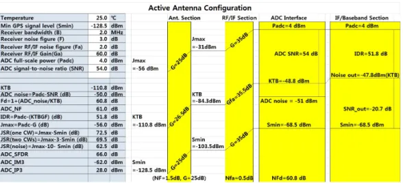
Fig. 1 shows the dynamic range of RF ASIC to be designed in the present study (Moulin et Al. 1998). To implement an anti-jamming function, the full-scale power of ADC (Padc) was set to 4 dBm, and the signal-to-noise ratio (ADC SNR) was set to 54 dB. In the environment shown in Fig. 1, KTB is -110.8 dBm, and the ADC output (noise out) has a value of -47.8 dBm due to the gain and noise characteristics of the antenna and the RF/IF end. In this regard, KTB is the reference thermal noise of IF bandwidth (B) at a room temperature (T=290 K), and K is the Boltzmann constant.
Therefore, the dynamic range of the designed RF ASIC was 51.8 dB (IDR = Padc - Noise out), and the jamming-to-signal ratio (JSR) (one CW) was 72.5 dB.
2.2 Design of High-Sensitivity/High-Resolution RF ASIC
Fig. 2 shows the functional block diagram of the high-
sensitivity/high-resolution RF ASIC for the implementation
of an anti-jamming function. The RF ASIC consists of RF
front end, baseband filter that can adjust gain, fractional-N
phase-locked-loop (PLL), high-speed 14-bit ADC, and
ADC sampling clock generation part. The RF ASIC has two
channels; and each channel has a bandwidth of 2~24 MHz
for the GPS L1/L2/L5 bands (1575.42/1227.6/1176.45 MHz),
a bandwidth of 14/22 MHz for the GLONASS L1/L2 bands
(1602.0/1246.0 MHz), and a bandwidth of 32/28 MHz for
the GALILEO E1/E5A bands (1575.42/1176.45 MHz). Also,
it was designed to have a wide dynamic range by applying
high-resolution ADC, RF attenuation block, and variable
gain mode low-noise amplifier (LNA). For the output signal
of the ADC, Low-Voltage Differential Signaling (LVDS)
was applied in order to reduce power consumption and
Fig. 1. Design of the dynamic range of RF ASIC.
to improve noise characteristics. To maintain isolation between each block, low-dropout (LDO) was separately implemented for each channel and block.
2.2.1 RF Front-End and Baseband Filter
In general, a GNSS receiver needs to receive signals that are lower than thermal noise, and thus it should have low-noise characteristics. Also, linearity is also very important for implementing an anti-jamming function.
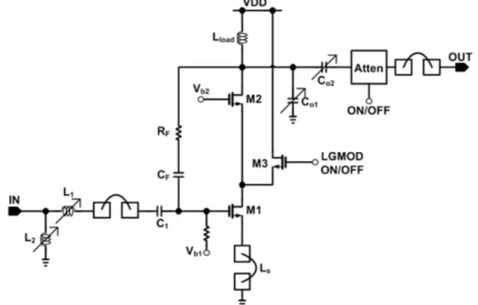
Fig. 3 shows the structure of cascode type LNA, and the feedback components RF and CF play a role in expanding the frequency characteristics. To achieve noise and input matching in LNA at the same time, the conventional inductive source degeneration technique was used. To optimize noise figure, external input matching networks (L1 and L2) need to be properly selected. The input side transistor (M1) provides bias through the internal constant current reference. When a very large jamming signal is introduced, LNA is operated in a low-gain mode by operating M3 in Fig. 3, and saturation of the RF front end is prevented by operating the RF attenuation block. When it is operated in a low-gain mode, a low noise figure can be obtained without affecting the input/output impedance.
Also, by integrating the RF attenuation block, a burden for the linearity of the next end mixer can be reduced.
The input impedance of the front-end mixer was set to 50 Ω in order to enable the connection of an external SAW filter. The input of the mixer was implemented based on common-source (CS) and common-gate (CG) stage in order to convert a single-ended signal into a differential signal while having a wide frequency band.
The baseband amplifier (BBA) consists of 7th order
Butterworth filter, programmable amplifier, output buffer, and DCOC subloop. The dynamic range of the baseband was implemented to have a value of -12 ~ 52 dB in order to include all the GNSS bands.
2.2.2 Fractional-N Frequency Synthesizer
Each band of the GPS, GLONASS, and GALILEO systems has different frequencies, and thus a frequency synthesizer should include all these bands. For this purpose, a broadband frequency resonant circuit is needed in one VCO and LC-VCO. To make a simple circuit, reduce the area of silicon, and implement a broadband frequency resonator, switched capacitor topology was used. Thus, LC-VCO including 7-bits capacitor banks was designed, and the AFC technique was used (Ko et al. 2005). AFC consists of three blocks: coarse tuning, fine tuning, and dividing blocks. The coarse tuning block corrects VCO frequency using a binary search algorithm. In this regard, an optimal capacitor bank code is searched by comparing the intermediate capacitor bank and the target frequency. To reduce the time for coarse tuning, a binary search algorithm is used. When coarse tuning is completed, the fine tuning block performs tuning based on typical PLL. The proposed VCO has a frequency band of 1.95 ~ 3.45 GHz.
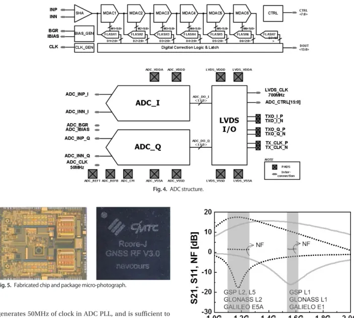
2.2.3 14-Bit ADC
Major performance factors for the implementation of an anti-jamming function include the dynamic range, resolution, and noise characteristics of ADC. In this study, ADC with a 14-bit resolution and a bandwidth of 50MHz was designed and implemented.
The RF front-end has a direct conversion structure, and
thus the Nyquist sampling clock of the ADC becomes half
of the low-IF structure. The RF ASIC designed in this study
Fig. 2. The proposed 2-channel GNSS receiver architecture.
generates 50MHz of clock in ADC PLL, and is sufficient to be used as a sampling clock and to satisfy the GNSS signal band with a maximum of 24 MHz.
ADC consists of sample-and-holder (S/H), pipe- line stages, bias block, clock generator, and digital error correction logic block. The input of the ADC was implemented based on a clock bootstrapping switch in order to reduce total harmonic distortion (Fayomi et al.
2004). Fig. 4 shows the ADC structure designed in this study.
To implement 14bit resolution and low power consumption, MDAC with a scaling stage structure of 3-3-3-3-3-3-2 was selected. Also, each ADC stage provides digital code for error correction.
3. RF ASIC MEASUREMENT RESULT
The designed RF ASIC was manufactured in a standard 0.18-μm complementary metal-oxide semiconductor
Fig. 4. ADC structure.
Fig. 5. Fabricated chip and package micro-photograph.
Fig. 6. The measured S-parameter and noise figure of LNA.
Fig. 7. The measured full-chain gain and NF of RF ASIC.
IIP3 was -7.5 dBm when there was a jamming signal. Also, the dynamic range of the BBA was between -12 dB and 52 dB, and the gain can be adjusted at a 1 dB step. The VCO was between 1.95 GHz and 3.45 GHz, and the tuning range
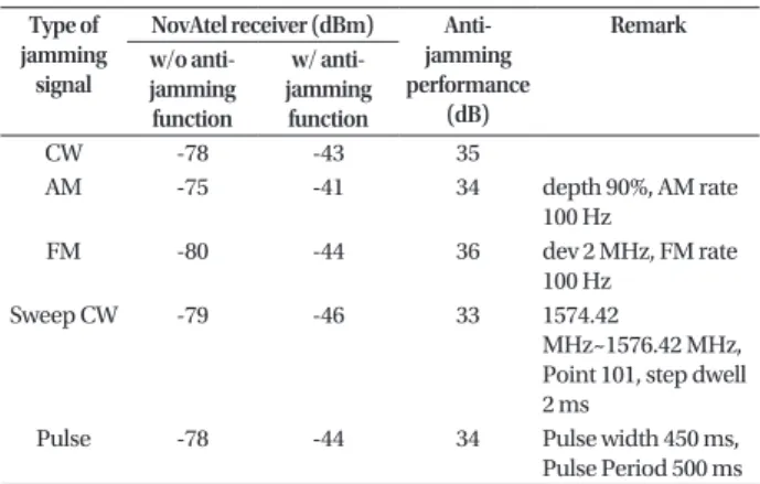
jamming function using RF ASIC was implemented as shown in Fig. 10, and the performance was verified. When general RF parts are used, seven to eight chip parts are needed for each channel, and additional matching circuits
Fig. 9. The measured output frequency range of VCO.
Fig. 8. The measured dynamic range of BBA.
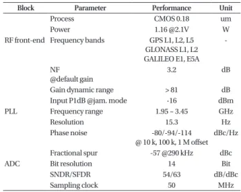
Table 1. Performance summary of RF ASIC.
Block Parameter Performance Unit