A Study on the Dielctric Properties of the PTC BaTiO 3 Ceramic Thin Films
Ik-Tae Im* and Byung Moon So
†*Dept. Mechanical Design Engineering, College of Eng., Chonbuk National University
†
Dept. IT Applied System Engineering, College of Eng., Chonbuk National University
ABSTRACT
The films were deposited at evaporator system and were annealed at heat treatment. The films had a dense microstructure with fine grains. The electrical properties of the films were dramatically controlled with annealing. Samples Preparation were analyzed in term of positive temperature coefficient of Resistivity Samples were made in the substrate tempera-true of 400
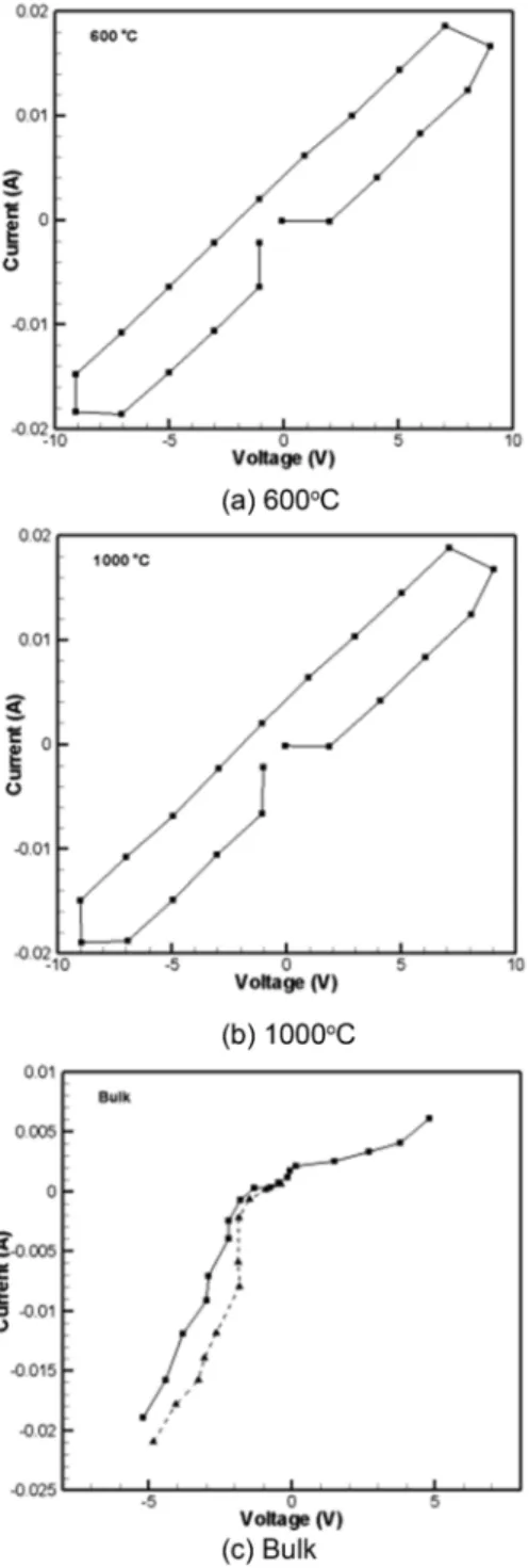
oC deposition time of 10 hours, and forward power of 210watt. R-T(resistivity-temperature) Characteristics of the samples were investigated as a function of the substrate type and the ambient temperature. The resistivity of the thin film specimens was compared with that of the bulk type specimens. By using RF/DC magnetron sputtering system, we obtained lower resistivity in the thermistor with thin BaTiO
3film than that in the bulk type thermistor.
Key Words : BaTiO
3, Thin Film, PTC
1. Introduction
Ceramic materials with very high electrical and thermal characteristics are widely studied due to the rapid growth of electronics industries including semi- conductor, personal computers and robots. Thin film technology is considered as one of the candidates to overcome the difficulties such as cost, volume and weight of chips and performance arisen to the devel- opment of electronic chips.
Thin films of Perovskite materials such as BaTiO
3[1-3] SrTiO
3and LiNbO have been tried using various techniques including evaporation, sput- tering, plasma enhanced chemical vapor deposi- tion[8], laser ablation, sol-gel process, hydrothermal process, molecular beam epitaxy and screen printing, and applied to thermistors capacitors, integrated optics, solid state display, FET nonvolatile memory and high frequency transducers.
Lots of studies have been devoted to find the possi- bility of thin film thermistor which uses the grain boundary in principle but it has not been fully under- stood. Thin film positive temperature coefficient ther-
mistor was first proposed by Feldman[4] in 1954. He used evaporation in vacuum to deposit BaTiO
3thin films. After his study, BaTiO
3thin films were depos- ited from various techniques such as using solu- tion[5], DC sputter[6] and RF sputter[7]. PTC semiconducting film was achieved by adding Y
2O
3into BaTiO
3in 1972. Thin films having PTC charac- teristics could be obtained from the optimized process conditions in case of RF sputter. However, it is diffi- cult to use the PTC films in mass production chips because of its high electrical resistivity.
In order to obtain good electrical characteristics, SiO
2is added to BaTiO
3for fabricating PTC thermistor in this study. The optimum process conditions of RF/
DC magnetron sputtering were found at first, and then thin films of BaTiO
3with SiO
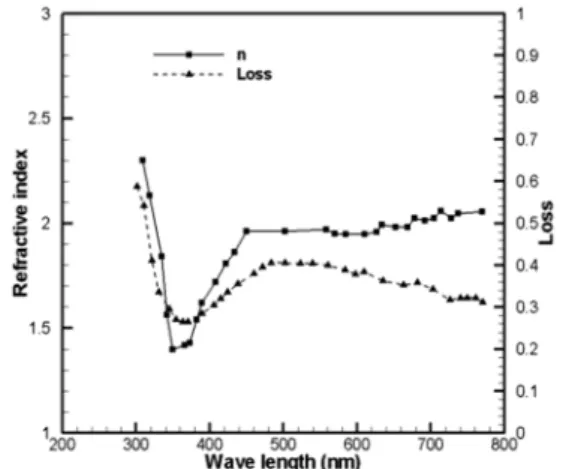
2PTC thermistor were deposited from the optimized conditions. The electrical characteristics and dielectric constants according to the wave length were investigated. The films were heat treated before measuring the characteristics.
2. Experiments
2.1. Targets and thin films
Targets were prepared to obtain desired composi-
†E-mail : [email protected]