1. 서 론
Transparent conductive electrodes(TCEs)는 터치 스 크린 패널[1, 2], 태양전지[3, 4], 발광 다이오드[5, 6]
와 같은 광전자 장치에서 주목받고 있는 재료라고 알려져 있다. 광학적 투명성 및 전기 전도성은 고성 능의 광전자 장치를 실현하기 위해 TCEs가 가져야
* Corresponding Author: Choong-Heui Chung Hanbat National University
Tel: +82-42-821-1277 E-mail: [email protected]
하는 가장 중요한 특성이다. 이러한 조건을 갖춘 TCEs 재료로 Indium tin oxide(ITO)가 대표적이지만 indium이 가지는 원료 자체의 문제, 고비용 제작 방 식 때문에 ITO를 대체하기 위한 재료의 연구가 필 수적이다. 이러한 ITO의 단점을 보완하며 나아가 대체할 수 있는 재료로 그래핀, 탄소나노튜브, 금속 나노와이어 등이 연구되고 있다. 그 중에서도 은 나 노와이어를 기반으로 하는 TCEs는 우수한 전기 전 도성, 광학적 투명성으로 인하여 ITO를 대체하여 다양한 차세대 광전자 응용 분야의 필수 구성 요소 로 각광받고 있다[7, 8, 9, 10, 11, 12, 13, 14, 15]. 일
<연구논문>
ISSN 2288-8403(Online) https://doi.org/10.5695/JKISE.2020.53.4.182
Shear-coating을 사용한 은 나노와이어 투명 전극 제조 및 특성 분석
조경수1, 홍기하2, 박준식1,2, 정중희1,2,*
1한밭대학교 공과대학 소재시스템공학과, 2한밭대학교 공과대학 신소재공학과
Preparation and characterization of
silver nanowire transparent electrodes using shear-coating
Kyung Soo Cho1, Ki-Ha Hong2, Joon Sik Park1,2, and Choong-Heui Chung1,2,*
1Department of Materials and Manufacturing Engineering, Hanbat National University, Daejeon 34158, Korea
2Department of Materials Science and Engineering, Hanbat National University, Daejeon 34158, Korea (Received 23 July, 2020 ; accepted 26 Aug, 2020)
Abstract7)
Indium tin oxide (ITO) used a transparent electrode of a photoelectric device has a low sheet resistance and a high transmittance. However, ITO is disadvantageous in that the process cost is expensive, and the process time is long. Silver nanowires (AgNWs) transparent electrodes are based on a low cost solution process. In addition, it has attracted attention as a next-generation transparent electrode material that replaces ITO because it has similar electrical and optical characteristic to ITO, it is noted as a. AgNW thin films are mainly produced by spin-coating. However, the spin-coating process has a disadvantage of high material loss. In this study, the material loss was reduced by using about 2∼10 ㎕ of AgNW solution on a (25
× 25) mm2 substrate using the shear-coating method. It was also possible to align AgNWs in the drag direction by dragging the meniscus of the solution. The electro-optical properties of the AgNW thin film were adjusted by changing the experimental parameters that the amount of AgNWs suspension, the gap between the substrate and the blade, and the coating speed. As a result, AgNW thin films with a transmittance of 90.7 % at a wavelength of 550 nm and a sheet resistance of 15 Ω/□ was deposited and exhibited similar properties to similar AgNW transparent electrodes studied by other researchers.
Keywords : Transparent conductive electrodes; Silver nanowires; Shear-coating; Alignment; Meniscus
반적으로 NWs TCE는 용액공정을 기반으로 하는 spin-coating 방법을 주로 사용하고 있으며, 이는 공 정 시간과 비용이 절감되는 장점을 갖는다고 알려 져 있다[16, 17]. 그러나 spin-coating 공정은 재료 손 실이 크다는 단점을 가지고 있다[18, 19]. 이러한 spin-coating 공정의 단점을 극복하기 위한 공정으로 spray-coating[20], bar-coating[21, 22] 등이 있다. 본 연구에서는 shear-coating 공정을 사용하여 재료 손 실 절감하였으며 동시에 단방향의 AgNWs 박막을 제조하였다. 단방향으로 배열된 AgNWs는 무작위 로 배열된 AgNWs에 비해 뛰어난 전기적 광학적 특 성을 얻을 수 있다고 알려져 있다[23]. Shear-coating 공정은 2개의 기판 사이에 포획된 AgNWs 현탁액 의 meniscus를 기판 끝까지 끌고 감으로써 기판 상 에 정렬된 AgNWs 박막을 제조하는 방법으로 실험 공정 변수인 AgNWs 현탁액의 양, 기판과 블레이드 사이의 거리와 코팅 속도를 조정해가며 AgNWs 박 막의 전기적 광학적 특성을 조절하였다. 또한 AgNWs 네트워크를 단방향 혹은 직교 방식으로 제 조하여 AgNWs 박막의 전기적 광학적 특성을 분석 하였으며 이는 AgNWs를 정렬하기 위한 다양한 공 정들과 비슷한 연구 결과를 나타냈다.
2. 실험 방법
유리 기판(25 mm × 25 mm × 1mm)을 아세톤, 에 탄올, 초 준수 물에서 각각 10분씩 초음파 세정하였 다. 하부 기판 상에 0.1 % poly-L-lysine (PLL) 용액 을 4000 rpm 속도로 60초 동안 스핀 코팅하여 기판 표면을 전처리하였다. 여기서 PLL 용액은 아민 작 용기로부터의 정전기력이 발생하여 기판에 대한 AgNWs의 접착력이 향상한다고 알려져 있다[24].
그 후 직경 40 ㎚, 길이 40 ㎛의 AgNWs(ACS Material, AgNw 40Eth-0.5g) 용액을 2.5 mg/ml의 농 도로 에탄올에 희석하여 사용하였다. Shear-coating 기구는 AgNWs 현탁액을 상온의 스테이지에서 제 어된 전단 속도로 코팅하도록 설계 및 제작되었다 [25]. 기판은 진공에 의해 상온의 하부 스테이지에 고정되고 상부 블레이드는 전동 스테이지에 의해 고정되어 기판에 대해 전단되도록 설계되었다. 상 부 유리 블레이드와 하부 기판 사이의 거리는 나사 에 의해 조정하였으며 고정한 거리에서 코팅된 기 판의 상태에 따라 거리를 변화하였다. 두 기판 사이 의 좁은 틈에 주입된 AgNWs 현탁액은 모세관 반응 에 의해 포획되었다. 그 후 전단 속도를 조정하여 하부 기판 상에 AgNWs 박막을 코팅하였으며 코팅
후 기판의 상태에 따라 전단 속도를 변화하였다. 그 후 기판 상에 AgNWs 현탁액의 용매를 건조하고 그 에 수직한 방향으로 동일한 코팅 조건을 수행하여 교차 정렬된 AgNWs 박막을 제조하였다. 코팅된 AgNWs의 저항을 감소하기 위하여 140 ℃에서 5분 동안 열처리하였다. 제조된 모든 AgNW TCEs는 UV-Vis spectrometer를 사용하여 깨끗한 유리 기판 을 기준으로 광학적 특성을 측정하였고 4-point probe를 사용하여 전기적 특성을 측정하였다.
3. 결과 및 고찰
그림 1(a∼d) 는 AgNWs 박막을 제조하는 shear- coating 방법의 개략도를 보여준다. 매우 적은 양의 AgNWs 현탁액은 진공으로 고정된 상부 유리 블레 이드와 하부 기판 사이의 틈에 위치한다. 모세관 작 용으로 인해 AgNWs 현탁액을 포획하여 기판에 대 한 meniscus를 형성하였다 (그림 1(a)). 그 후 하부 기판에 대해 상부 유리 블레이드를 이동하여 AgNWs 박막을 형성하였다. 이때 상부 유리 블레이 드가 이동할 때 meniscus에서 AgNWs에 가해지는 전단 응력에 의해 AgNWs는 전단력의 방향을 따라 정렬하였다 (그림 1(b)). AgNWs 박막이 코팅된 기 판을 90˚회전시키고 (그림 1(c)), 그 위에 AgNWs를 추가로 코팅하였다 (그림 1(d)). 그림 1(e)는 (25 × 25) mm2 유리 기판 상에 shear-coating 공정을 준비 중인 사진이다. 하부 기판과 상부 블레이드 사이에 형성된 AgNWs 현탁액의 meniscus가 형성되었음을 확인할 수 있다. 이때 AgNWs에 가해지는 전단력에 영향을 미치는 AgNWs 현탁액의 양, 기판과 블레이 드 사이의 거리, 코팅 속도를 공정 변수로 하여 이 에 따른 AgNWs의 정렬 정도를 연구하였다.
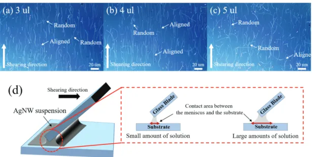
먼저 기판과 블레이드 사이에 주입되는 AgNWs 현탁액의 양에 따른 NWs의 정렬 정도를 조사하였 다. 그림 2(a∼c)는 주입되는 AgNWs 현탁액의 양에 따른 AgNWs 박막의 표면 형상을 보여주는 광학현 미경 이미지이다. 이때 정렬된 AgNWs를 ‘Aligned’
라 표시라고 오정렬한 AgNWs를 ‘Random’이라 표 시하였다. 그림 2(a∼c)는 각각 3 ㎕, 4 ㎕, 5 ㎕의 AgNWs 현탁액을 주입하여 코팅한 샘플이다. 그림 2(a∼c)에서 볼 수 있듯이 주입량이 증가할수록 오 정렬한 AgNWs가 증가하였으며 주입량이 감소할수 록 AgNWs가 코팅 방향에 따라 정렬하였다. 이것은 주입된 AgNWs 현탁액의 양이 증가할수록 대부분 의 AgNWs에 가해지는 전단력이 약해지기 때문이
Fig. 2. (a∼c) Optical microscopy images of samples shear-coated on substrates with different injection rates. (d) Schematic showing the NW alignment mechanism according to the amount of AgNWs suspension injected. As the amount of suspension increases, the contact area between the substrate and meniscus increases, so the probability of misalignment of AgNWs located far from the blade increases.
Fig. 1. (a∼d) Schematic of manufacturing an aligned AgNWs thin film using a shear-coating process. (e) Photo after injection of AgNWs suspension during the actual shear-coating process.
A suspension meniscus was formed between the substrate and the blade.
다. AgNWs의 현탁액이 증가할수록 기판과 블레이 드 사이의 meniscus 두께와 접촉 면적이 증가하게 되는데 기판과 meniscus의 접촉 면적이 증가하면 블
레이드와 멀리 떨어진 위치의 AgNWs에 가해지는 전단력은 약하기 때문에 정렬도가 감소하게 된다 (그림 2(d)).
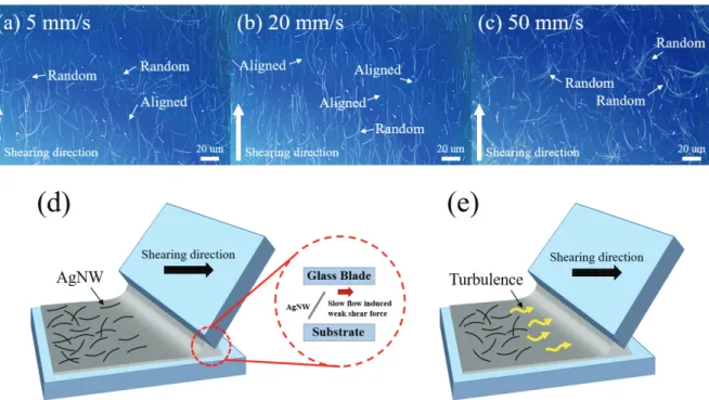
Fig. 4. NW alignment mechanism according to coating speed. (a∼c) Optical microscopy images of samples shear-coated on substrates with different coating speeds. (d) When the coating speed is slow, weak shear force does not induce AgNWs rotation. (e) When the coating speed is fast, turbulence will occur in the AgNWs suspension layer, reducing the unidirectional properties of AgNWs.
Fig. 3. (a∼c) Optical microscopy images of samples shear-coated on substrates with different gaps
between the substrate and the blade. (d) Schematic showing the NW alignment mechanism according to
the gap between the substrate and the blade. When the gap is large, the alignment potential is high
because the AgNWs located near the blade having a strong shear force. On the other hand, AgNWs
located far from the blade increases the possibility of misalignment because the shear force is weak.
다음은 공정 변수 중 기판과 블레이드 사이의 거 리에 따른 NWs의 정렬 정도를 조사하였다. 그림 3(a∼c)는 기판과 블레이드 사이 거리에 따른 AgNWs 박막의 표면 형상을 보여주는 광학현미경 이미지이다. 여기서 기판과 블레이드 사이의 거리 는 각각 10 ㎛, 30 ㎛, 80 ㎛이고 마찬가지로 정렬된 AgNWs와 오정렬된 AgNWs를 각각 ‘Aligned’,
‘Random’이라고 표시하였다. 동일한 양의 AgNWs 현탁액이 주입되었을 때, 기판과 블레이드 사이의 거리가 매우 가까울수록 기판과 meniscus의 접촉 면 적이 증가하고 앞서 설명했듯이 결국 AgNWs의 정 렬도가 감소한다(그림 3(a)). 그림 3(b)가 그림 3(c) 에 비해 바람직하게 정렬된 AgNWs 박막을 형성하 였다. 이것은 기판과 블레이드 사이의 거리에 대한 meniscus의 높이(δ) 변화에 따른 전단력의 세기 분 포로 설명할 수 있다(그림 3(d)). 블레이드를 이동시 키는 동안 전단력 구배는 Couette flow에서 meniscus 높이의 함수로서 생성된다[26, 27]. 따라서 블레이 드에서 멀리 위치한 AgNWs는 전단력이 감소하여 오정렬 가능성을 증가시킨다[28, 29]. 그림 3(d)에서 볼 수 있듯이 두꺼운 meniscus에서는 다수의 AgNWs가 블레이드에 멀리 위치하여 오정렬 가능 성이 높은 반면에 얇은 meniscus에서는 대부분의 AgNWs가 블레이드 근처에 위치하기 때문에 정렬 가능성이 높다.
위에서 언급한 공정 변수 중 코팅 속도에 따른
NWs 정렬 정도를 조사하였다. 그림 4(a∼c)는 코팅 속도에 따른 AgNWs 박막의 표면 형상을 보여주는 광학현미경 이미지이다. 이때 코팅 속도는 각각 5 mm/s, 20 mm/s, 50 mm/s이고 다양한 코팅 속도 조 건 중 그림 4(b)에서 가장 바람직한 정렬된 AgNWs 박막을 형성하였다. 그 이유는 코팅 속도가 전단력 의 세기 변화와 코팅된 AgNWs 현탁액 층에 미치는 영향 때문이다(그림 4(d, e)). 코팅 속도가 너무 느리 면 전단력의 크기가 약하기 때문에 AgNWs가 정렬 되지 못할 뿐만 아니라 AgNWs 현탁액의 용매인 에 탄올이 계속해서 증발하기 때문에 AgNWs 현탁액 이 기판의 끝부분까지 도달하지 못한다. 따라서, 기 판의 처음과 끝에 코팅되는 AgNWs의 양이 달라지 게 된다 (그림 4(d)). 또한 블레이드의 이동속도가 너무 빠르면 그림 4(e)에서 볼 수 있듯이 코팅된 상 태의 AgNWs 현탁액 층에서 난류가 발생하여 AgNWs의 정렬도를 크게 감소시킨다.
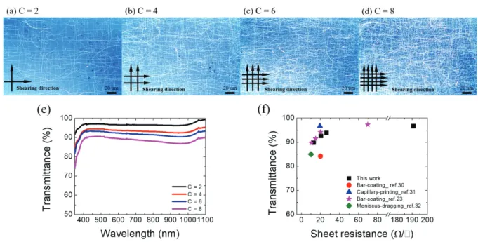
Shear-coating 공정의 공정 변수 중 바람직한 AgNWs 정렬의 특성을 보여주는 조건들을 사용하 여 기판에 직교 방향으로의 코팅을 수행하였다(그 림 5(a∼d)). 여기서 C = 2, C = 4, C = 6, C = 8은 직교 방향으로 코팅한 수를 표시한 것으로 각각 2 회, 4회, 6회, 8회 코팅하였다. 그림 5(a∼d)에서 볼 수 있듯이 교차 정렬된 AgNWs 박막은 증착 수가 증가할수록 AgNWs의 밀도가 증가한다. 따라서 AgNWs 박막의 광학 투과율은 C가 증가함에 따라
Fig. 5. (a∼d) Optical microscopy image coated orthogonally to the substrate using desirable AgNWs alignment conditions during the shear-coating process. The number of coatings was 2, 4, 6 and 8 times, and was expressed as C = 2, 4, 6, 8. (e) Transmittance graph of the shear-coating AgNW thin films.
Decrease gradually as C increases. (f) A graph comparing the electro-optical properties of various process
methods for making aligned AgNW thin films.
점진적으로 감소하였다 (그림 5(e)). 그림 5(e)는 교 차 정렬된 AgNWs 박막의 높은 광학 투과율을 보여 주는 그래프로 550 nm 파장에서 각각 96.7 %, 93.9
%, 92.6 %, 89.8 % 투과도를 나타내고, 이때 측정되 는 샘플의 면저항은 각각 190.8 Ω/□, 26.4 Ω/□, 20.5 Ω/□, 12.79 Ω/□이다. 따라서 교차 코팅 수가 증가할수록 광학 투과율이 낮지만 전기 전도성과 밀도가 높고 투명 전극을 얻을 수 있었다. 그림 5(f) 는 다양한 공정 방법들을 사용하여 정렬된 AgNW TCEs의 전기적 광학적 특성을 비교한 그래프이다.
Shear-coating을 사용하여 교차 정렬한 AgNWs(550 nm에서의 투과도 93.9 %∼89.8 %에서 면저항 26.4 Ω/□∼12.79 Ω/□)는 capillary-printing 공정으로 교 차 정렬한 AgNWs(550 nm에서의 투과도 96.7 %에 서 면저항 19.5 Ω/□)[31]에 비해 비교적 떨어진 특 성을 보였으나 bar-coating 공정으로 교차 정렬한 AgNWs(550 nm에서의 투과도 84.2 %에서 면저항 20 Ω/□, 97.3 %∼89.8 %에서 면저항 69.7 Ω/□∼
10.4 Ω/□)[30,23], meniscus-dragging 공정으로 교차 정렬한 AgNWs(550 nm에서의 투과도 85 %에서 면 저항 10 Ω/□)[32]와 유사하거나 우수한 특성을 보 였다.
4. 결 론
본 연구에서는 shear-coating 공정을 사용하여 재 료 손실을 절감하였으며 동시에 단방향의 AgNWs 박막을 제조하였다. 이때 실험 공정 변수인 AgNWs 현탁액의 양, 기판과 블레이드 사이의 거리, 코팅 속도를 조정해가며 NWs에 가해지는 전단력이 NWs 의 정렬도에 미치는 영향을 조사하였다. 먼저 AgNWs 현탁액의 주입량에 따른 기판과 meniscus의 접촉 면적으로 인한 전단력에 의해 NWs 정렬도가 결정되었다. 두 번째로 기판과 블레이드 사이의 거 리는 meniscus 두께에 의한 전단력 구배에 의해 NWs 정렬도가 결정되었다. 마지막으로 코팅속도는 너무 느리면 전단력이 약해지지만 너무 빠르면 코 팅된 AgNWs 현탁액 층에서 난류가 발생하였다. 공 정 변수의 바람직한 코팅 조건으로 AgNWs 네트워 크를 단방향 혹은 직교 방식으로 제조하여 AgNWs 박막의 전기적 광학적 특성을 분석하였다. 결론적 으로 재료 손실을 절약하여 간단하고 저렴한 shear-coating 공정으로 제조한 AgNW TCEs는 AgNWs를 정렬하기 위한 다양한 공정들과 비슷한 연구 결과를 나타냈다.
References
[1] S. Bae, H. Kim, Y. Lee, X. Xu, J. -S. Park, Y.
Zheng, J. Balakrishnan, T. Lei, H. R. Kim, Y. I.
Song, J. -J. Kim, K. S. Kim, B. Özyilmaz, J. H.
Ahn, B. H. Hong, S. Iijima, Roll-to-roll production of 30-inch graphene films for transparent electrodes, Nat. Nanotechnol., 5 (2010) 574-578.
[2] H. Wu, D. Kong, Z. Ruan, P. -C. Hsu, S.
Wang, Z. Yu, T. J. Carney, L. Hu, S. Fan, Y.
Cui, A transparent electrode based on a metal nanotrough network, Nat. Nanotechnol., 8 (2013) 421-425.
[3] M. Kaltenbrunner, M. S. White, E. D. Głowacki, T. Sekitani, T. Someya, N. S. Sariciftci, S.
Bauer, Ultrathin and lightweight organic solar cells with high flexibility, Nat. Commun., 3 (2012) 550.
[4] H. Kang, S. Jung, S. Jeong, G. Kim, K. Lee, Polymer-metal hybrid transparent electrodes for flexible electronics, Nat. Commun., 6 (2015) 1-7.
[5] T. H. Han, Y. Lee, M. -R. Choi, S. -H. Woo, S. -H. Bae, B. H. Hong, J. -H. Ahn, T. -W.
Lee, Extremely efficient flexible organic light-emitting diodes with modified graphene anode, Nat. Photonics, 6 (2012) 105–110.
[6] N. Li, S. Oida, G. S. Tuleski, S. -J. Han, J. B.
Hannon, D. K. Sadana, T. -C. Chen, Efficient and bright organic light-emitting diodes on single-layer graphene electrodes, Nat. Commun., 4 (2013) 1-7.
[7] S. Lee, J. Jang, T. Park, Y. M. Park, J. S. Park, Y. -K. Kim, H. -K. Lee, E. -C. Jeon, D. -K.
Lee, B. Ahn, C. -H. Chung, Electrodeposited Silver Nanowire Transparent Conducting Electrodes for Thin-Film Solar Cells, ACS Appl.
Mater. Interfaces, 12 (2020) 6169-6175.
[8] S. Lee, K. S. Cho, S. Song, K. Kim, Y. J. -Eo, J. H. Yun, J. Gwak, C. -H. Chung, Fabrication of robust nanoscale contact between a silver nanowire electrode and cds buffer layer in cu(In,ga)se2 thin-film solar cells, J. Vis. Exp., (2019) 2-7.
[9] H. Ji, J. Jang, S. Lee, C. -H. Chung, Enhancement of electrical conductivity in silver nanowire
network for transparent conducting electrode using copper electrodeposition, Korean J. Mater.
Res., 29 (2019) 311-316.
[10] S. Lee, J. S. Lee, J. Jang, K. -H. Hong, D. -K.
Lee, S. Song, K. Kim, Y. -J. Eo, J. H. Yun, J.
Gwak, C. -H. Chung, Robust nanoscale contact of silver nanowire electrodes to semiconductors to achieve high performance chalcogenide thin film solar cells, Nano Energy, 53 (2018) 675- 682.
[11] J. Jang, D. -Y. Park, K. -H. Hong, S. Song, K.
Kim, Y. -J. Eo, J. Gwak, J. H. Yun, C. -H.
Chung, Improvement of Contact Resistance Between Each Silver Nanowire and Thermal Stability of Silver Nanowire Transparent Electrodes by Electrodeposition, Nanosci.
Nanotechnol. Lett., 10 (2018) 528-532.
[12] J. Jang, J. S. Lee, K.H. Hong, D.K. Lee, S.
Song, K. Kim, Y. J. Eo, J. H. Yun, C.H.
Chung, Cu(In,Ga)Se2 thin film solar cells with solution processed silver nanowire composite window layers: Buffer/window junctions and their effects, Sol. Energy Mater. Sol. Cells, 170 (2017) 60-67.
[13] B. Bob, A. Machness, T. -B. Song, H. Zhou, C.
-H. Chung, Y. Yang, Silver nanowires with semiconducting ligands for low-temperature transparent conductors, Nano Res., 9 (2016) 392- 400.
[14] C. -H. Chung, T. -B. Song, B. Bob, R. Zhu, Y.
Yang, Solution-processed flexible transparent conductors composed of silver nanowire networks embedded in indium tin oxide nanoparticle matrices, Nano Res., 5 (2012) 805- 814.
[15] C. -H. Chung, T. -B. Song, B. Bob, R. Zhu, H.
-S. Duan, Y. Yang, Silver nanowire composite window layers for fully solution-deposited thin-film photovoltaic devices, Adv. Mater., 24 (2012) 5499-5504.
[16] D. S. Leem, A. Edwards, M. Faist, J. Nelson, D. D. C. Bradley, J. C. De Mello, Efficient organic solar cells with solution-processed silver nanowire electrodes, Adv. Mater., 23 (2011) 4371–4375.
[17] S. Bae, H. Kim, Y. Lee, X. Xu, J. -S. Park, Y.
Zheng, J. Balakrishnan, T. Lei, H. R. Kim, Y. I.
Song, J. -J. Kim, K. S. Kim, B. Özyilmaz, J. H.
Ahn, B. H. Hong, S. Iijima, Roll-to-roll production of 30-inch graphene films for transparent electrodes, Nat. Nanotechnol., 5 (2010) 574–578.
[18] Y. Lee, S. -Y. Min, T. -S. Kim, S. -H. Jeong, J. Y. Won, H. Kim, W. Xu, J. K. Jeong, T.
-W. Lee, Versatile Metal Nanowiring Platform for Large-Scale Nano- and Opto-Electronic Devices, Adv. Mater., 28 (2016) 9109-9116.
[19] H. Koga, M. Nogi, N. Komoda, T. T. Nge, T.
Sugahara, K. Suganuma, Uniformly connected conductive networks on cellulose nanofiber paper for transparent paper electronics, NPG Asia Mater., 6 (2014) 1-8.
[20] J. -H. Choe, A. -Y. Jang, J. -H. Kim, C. -H.
Chung, K. -H. Hong, Effects of dispersion solvent on the spray coating deposition of silver nanowires, J. Korean Inst. Met. Mater., 55 (2017) 509-514.
[21] S. J. Lee, Y. -H. Kim, J. K. Kim, H. Baik, J.
H. Park, J. Lee, J. Nam, J. H. Park, T. -W.
Lee, G. -R. Yi, J. H. Cho, A roll-to-roll welding process for planarized silver nanowire electrodes, Nanoscale, 6 (2014) 11828-11834.
[22] H. Sim, S. Bok, B. Kim, M. Kim, G. -H. Lim, S. M. Cho, B. Lim, Organic-Stabilizer-Free Polyol Synthesis of Silver Nanowires for Electrode Applications, Angew. Chemie - Int.
Ed., 55 (2016) 11814-11818.
[23] S. Cho, S. Kang, A. Pandya, R. Shanker, Z.
Khan, Y. Lee, J. Park, S. L. Craig, H. Ko, Large-Area Cross-Aligned Silver Nanowire Electrodes for Flexible, Transparent, and Force-Sensitive Mechanochromic Touch Screens, ACS Nano, 11 (2017) 4346-4357.
[24] Q. Sun, S. J. Lee, H. Kang, Y. Gim, H. S.
Park, and J. H. Cho, Positively-charged reduced graphene oxide as an adhesion promoter for preparing a highly-stable silver nanowire film, Nanoscale, 7 (2015) 6798-6804.
[25] J. Choe, J. Song, D. Lee, H. R. Byun, M. S.
Jeong, C. -H. Chung, K. -H. Hong, J. Kim, Rapid large-grain (>100 μm) formation of organic-inorganic perovskite thin films via shear
deposition for photovoltaic application, Sol.
Energy, 191 (2019) 629-636.
[26] C. H. Choi and C. J. Kim, Large slip of aqueous liquid flow over a nanoengineered superhydrophobic surface, Phys. Rev. Lett., 96 (2006) 1-4.
[27] H. Yu, P. Zhang, A kinetic-hydrodynamic simulation of microstructure of liquid crystal polymers in plane shear flow, J. Nonnewton.
Fluid Mech., 141 (2007) 116-127.
[28] B. Park, I. G. Bae, Y. H. Huh, Aligned silver nanowire-based transparent electrodes for engineering polarisation-selective optoelectronics, Sci. Rep., 6 (2016) 1-9.
[29] D. M. Kuncicky, R. R. Naik, O. D. Velev, Rapid deposition and long-range alignment of nanocoatings and arrays of electrically conductive
wires from tobacco mosaic virus, Small, 2 (2006) 1462-1466.
[30] K. M. Chiang, Z. Y. Huang, W. L. Tsai, H. W.
Lin, Orthogonally weaved silver nanowire networks for very efficient organic optoelectronic devices, Org. Electron., 43 (2017) 15-20.
[31] S. Kang, T. Kim, S. Cho, Y. Lee, A. Choe, B.
Walker, S. -J, Ko, J. Y. Kim, H. Ko, Capillary printing of highly aligned silver nanowire transparent electrodes for high-performance optoelectronic devices, Nano Lett., 15 (2015) 7933-7942.
[32] Y. Ko, S. K. Song, N. H. Kim, S. T. Chang, Highly Transparent and Stretchable Conductors Based on a Directional Arrangement of Silver Nanowires by a Microliter-Scale Solution Process, Langmuir, 32 (2016) 366-373.