9-1 / Y. Park
• IMID 2009 DIGEST
Abstract
We have determined the electronic energy level alignment at the interface between 4,4’-bis-N-phenyl-1-naphthylamino biphenyl (NPB) and 1,4,5,8,9,11-hexaazatriphenylenehexacarbonitrile (HAT-CN) using ultraviolet photoelectron spectroscopy (UPS). The highest occupied molecular orbital (HOMO) of 20 nm thick HAT-CN film was located at 3.8 eV below the Fermi level. Thus the lowest unoccupied molecular orbital (LUMO) is very close to the Fermi level. The HOMO position of NPB was only about 0.3 eV below Fermi level at NPB/HAT-CN interface. This enables an easy excitation of electrons from the NPB HOMO to the HAT-CN LUMO, creating electron-hole pairs across this organic-organic interface. We also study the interaction of HAT-CN with a few metallic surfaces including Ca, Cu, and ITO using UPS and ab-inito electronic structure calculation techniques.
1. Introduction
Organic light emitting diodes (OLEDs) are becoming more and more attractive as the key ingredient for next generation display technology. [1] The rapid progress of the technology is evident in various portable consumer electronic devices employing OLED display panels. A typical OLED is composed of several thin layers of organic and inorganic materials. They include anode and cathode electrodes, an organic luminescent layer, and charge transport layers. In addition, higher OLED efficiency can be achieved by introducing and later improving electron injection layer [2–5] or hole injection layer. [6,7] Notably, the use of 1,4,5,8,9,11-hexaazatriphenylene-hexacarbonitrile (HAT-CN) as the connecting layer in some of the tandem OLEDs for higher power efficiency was successfully demonstrated recently, [8,9] in which the importance of the interface between HAT-CN and 4,4’-bis(N-phenyl-1-naphthylamino)biphenyl (NPB) was highlighted.
In this paper, we report the molecular energy level alignment between HAT-CN and NPB using UV photoelectron spectroscopy (UPS). The HAT-CN has recently been studied quite extensively although not in the context of the OLED applications. [10–14] The chemical structures of the molecules are shown in Figure 1. Our UPS data were measured while NPB was deposited on HAT-CN(20 nm)/Au film. They provide direct evidences that the lowest unoccupied molecular orbital (LUMO) of HAT-CN is either pinned at, or very close to, the Fermi level, while the highest occupied molecular orbital (HOMO) of NPB is only about 0.3 eV below the Fermi level at the interface. Such a small HOMO-LUMO offset allows the electrons and holes to be generated and separated at the interface when external bias voltage is applied, which is sometimes called charge carrier generation. These findings, together with the known properties of the molecules, allowed us to create a detailed energy level diagram at NPB/HAT-CN/Au interfaces.
2. Experimental
The UPS experiments were carried out in an ultrahigh vacuum chamber connected to a preparation chamber where all the deposition processes took place. Spectra were recorded on a VG ESCALAB 220i system using a He I (21.2 eV) source. The base
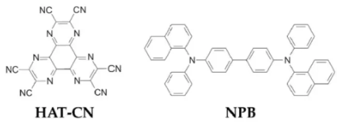
Fig. 1. The chemical structures of HAT-CN and NPB.
Energy Level Alignment between Hole Injecting HAT-CN
and Metals and Organics: UPS and
ab-initioCalculations
H. Kang
1, J. H. Kim
1, J. K. Kim
1, Y. K. Kwon
1, J. W. Kim
2, and Y. Park
11Dept. of Physics, Kyung Hee University, Seoul 130-701, Korea
Tel.:82-50-5252-0052, E-mail: [email protected]
2Korea Research Institute of Standards and Science, Deajeon 305-240, Korea
9-1 / Y. Park
IMID 2009 DIGEST • pressures of the preparation chamber and the analysis
chamber were 7 X 10⁻⁹ and 2 X 10⁻¹⁰ Torr,
respectively. The UPS spectra were recorded with a sample bias of -10 V. Energy resolutions were approximately 0.1 eV. The evaporation sources for NPB and HAT-CN were homemade thermal sources and installed in the preparation chamber. An Au foil was initially sputter cleaned with 3 keV Ar ion beam in the analysis chamber until pure Au valence spectra were obtained. The deposition rate was carefully monitored by using a quartz crystal microbalance and was typically 0.1 nm/min. All the measurements and depositions were done at room temperature. Due to the nature of the photoemission spectroscopy, all the measured energy levels are referenced to the Fermi level.
3. Results and discussion
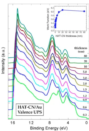
Figure 2 shows the evolution of the valence band spectra of HAT-CN sequentially deposited up to 80 nm onto Au substrate. The Fermi level cutoff of Au was evident at the binding energy (BE) of 0 eV, which gradually disappears as the HAT-CN thickness increases. The inset of Fig. 2 plots the changes in work function during the deposition process. Starting from Au work function of 5.2 eV, the maximum values observed for HAT-CN film were about 6.1 eV. This is oxides [15] and Re oxides. [7] The Au valence features including the Fermi edge and the peak at 2.6 eV completely disappeared only at about 20 nm of HAT-CN, which suggests that either the Au substrate is quite rough or the growth morphology of HAT-CN is not layer by layer. The process of Ar ion sputter cleaning of Au substrate may develop some roughness. It is worth noting that the 80 nm thick film of HAT-CN does not cause any charging effect on UPS spectra, in contrast to other common organic molecular materials such as Alq3 and NPB. It is known that Alq3 exhibits charging effect in UPS spectra above about 15–20 nm, while NPB starts charging just above 1.5 nm. Such a good charge conduction property of HAT-CN may be utilized to optimize the optical thickness of an OLED layer stack. In fact, it would be interesting to find various transport properties of this molecular film, such as temperature dependent conductivity and Hall coefficient.
At the early stages of HAT-CN on Au, it is difficult to locate the HOMO onset of the molecule due to the strong emissions from Au substrate. For thicker HAT-CN films, the HOMO position was clearly observed
Fig. 2. Evolution of the valence band spectra for HAT-CN/Au with increasing thickness. The inset shows the work function changes as measured by the change in secondary electron cutoff position.
and determined to be 3.8 eV. While the transport band gap of HAT-CN has not been precisely measured, the UV-visible absorption spectra exhibited onset at about 370 nm (3.35 eV) and a peak at 320 nm (3.88 eV). [9,13] These values suggest that the LUMO level is very close to the Fermi level, and as a consequence, the material would be a strong n-type. This is valid even after considering the fact that the optical gap is typically smaller than the transport gap in molecular solids.
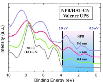
Figure 3 shows the evolution of the valence band spectra while NPB was gradually deposited on a 20 nm-thick HAT-CN film. As soon as the 0.4 nm of NPB was deposited, the HOMO onset could be clearly observed at about 0.3 eV. For NPB thickness of 1.5 nm, the HOMO position slightly moved toward the higher BE direction. Further deposition shifted the HOMO peak more than 0.5 eV. This movement of the HOMO peak could be due to the charging of the NPB films. To clarify this issue, we performed the time-dependent measurements of secondary electron cutoff positions. A comparison was made between the first measurements of UPS spectrum after NPB was
9-1 / Y. Park
• IMID 2009 DIGEST
Fig. 3. The valence band UPS data for thing NPB
on 20 nm HAT-CN. The HOMO onset position of the HAT-CN is clearly observed at3.8 eV, while that of NPB is at 0.3 eV. Thicker NPB layer exhibited charging
freshly deposited and the measurements made 20 min later while UV lamp was left turned on. The results indicated that the charging can be a significant factor for NPB films thicker than about 1.0 nm. The HOMO position of 10 nm thick film including the charging effect was about 1.0 eV.
The 0.3 eV HOMO position of NPB at the interface indicates that the electrons from the NPB HOMO can be easily excited to the HAT-CN LUMO. This process is a good reason for using HAT-CN as a layer between NPB and an anode where its actual role is generating electron-hole pairs at the interface with NPB and transporting them toward the anode. It can also be utilized as a highly efficient connecting layer in a tandem OLED as recently demonstrated. [8,9] In this respect the interface between HAT-CN and Au is not as important as copper phthalocyanine (CuPc)/indium tin oxide (ITO) interface in conventional structures such as NPB/CuPc/ITO, where the hole injection barrier between ITO and CuPc is very important. In addition, the most recent active matrix OLED panels are top-emission-type, some of which do not use the ITO. Instead, they use metallic substrates such as Ag for anode. Therefore, the properties of HAT-CN on metallic substrate are related to the practical device fabrication practices.
The findings made so far, together with values in the literature, allowed us to construct an energy level diagram for NPB/HAT-CN/Au interface as shown in Fig. 4. As mentioned earlier, the optical gap of HAT-CN measured with UV-visible absorbance [9,13] is
smaller than the measured HOMO position, which makes this material almost like a metallic conductor. If a molecule contains electron withdrawing functional groups, the electron affinity (EA) becomes larger. The presence of six nitrile groups (C≡N) in
HAT-CN guarantees this molecule to be a strong electron withdrawer. Therefore it is not surprising to find that the EA is large. In fact, the metallic nature of the hexagonally ordered monolayer of HAT-CN on Ag(111) was recently reported. [14] The LUMO derived states below Fermi level facilitate the charge transfer from the metallic surface, and the band associated with the HAT-CN LUMO is pinned right at the Fermi level of Ag(111). We believe it is unlikely that such a condition would continue with increasing HAT-CN film thickness. Therefore, we indicated in Fig. 4 that the LUMO offset is a value smaller than 0.1 eV. The crystal structure [10] of HAT-CN shows a weak intermolecular interactions avoiding _-_ stacking, which helps preserve large molecular EA in solids.
Fig. 3. The optical band gap of HAT-CN is less than 3.8 eV, although the transport LUMO level may not be below the Fermi level.
4. Summary
In summary, we studied the molecular energy level alignment between HAT-CN and NPB using UPS. While the work function of a 20 nm thick HAT-CN film deposited on Au is about 6.1 eV, it remained a good conducting molecular layer. Our data also clearly indicate that the LUMO of HAT-CN is very
9-1 / Y. Park
IMID 2009 DIGEST • close to the Fermi level and the HOMO of NPB is
located only about 0.3 eV below Fermi level at this molecular interface. This arrangement allows the electrons from the NPB HOMO to be easily excited to the HAT-CN LUMO, forming a charge carrier generation interface. A detailed energy level alignment diagram at the interface was constructed.
Acknowledgement
Y.P. acknowledges the supports of Korea Basic Science Institute (Grant No. N27038) and KRISS.
5. References
1. C. W. Tang and S. A. Van Slyke, Appl. Phys. Lett.
51, p.913 (1987).
2. S. A. Van Slyke, C. H. Chen, and C. W. Tang,
Appl. Phys. Lett.69, p.2160 (1996).
3. Y. Park, J. Lee, S. K. Lee, and D. Y. Kim, Appl. Phys. Lett.79, p.105 (2001).
4. J. Lee, Y. Park, S. K. Lee, E.-J. Cho, D. Y. Kim, H. Y. Chu, H. Lee, L.-M. Do, and T. Zyung, Appl. Phys. Lett.80, p.3123 (2002).
5. J. Lee, Y. Park, D. Y. Kim, H. Y. Chu, H. Lee, and L.-M. Do, Appl. Phys. Lett.82, p.173 (2003).
6. C.-C. Chang, M.-T. Hsieh, J.-F. Chen, S.-W. Hwang, and C. H. Chen, Appl. Phys. Lett. 89,
p.253504 (2006).
7. D.-S. Leem, H.-D. Park, J.-W. Kang, J.-H. Lee, J. W. Kim, and J.-J. Kim, Appl. Phys. Lett. 91,
p.011113 (2007).
8. L. S. Liao and K. P. Klubek, Appl. Phys. Lett. 92,
p.223311 (2008).
9. L. S. Liao, W. K. Slusarek, T. K. Hatwar, M. L. Ricks, and D. L. Comfort, Adv. Mater. (Weinheim, Ger.) 20, p.324 (2008).
10. P. S. Szalay, J. R. Galán-Mascarós, R. Clérac, and K. R. Dunbar, Synth. Met.122, p.535 (2001).
11. P. S. Szalay, J. R. Galán-Mascarós, B. L. Schottel, J. Bacsa, L. M. Pérez, A. S. Ichimura, A. Chouai, and K. R. Dunbar, J. Cluster Sci. 15, p.503
(2004).
12. S. Furukawa, T. Okubo, S. Masaoka, D. Tanaka, H.-C. Chang, and S. Kitagawa, Angew. Chem., Int. Ed.44, p.2700 (2005).
13. T.-H. Chang, B.-R. Wu, M. Y. Chiang, S.-C. Liao, C. W. Ong, H.-F. Hsu, and S.-Y. Lin, Org. Lett.7,
p.4075 (2005).
14. H. Glowatzki, B. Bröker, R.-P. Blum, O. T. Hofmann, A. Vollmer, R. Rieger, K. Müllen, E. Zojer, J. P. Rabe, and N. Koch, Nano Lett. 8,
p.3825 (2008).
15. H. Lee, S. W. Cho, K. Han, P. E. Jeon, C.-N. Whang, K. Jeong, K. Cho, and Y. Yi, Appl. Phys. Lett.93, p.043308 (2008).