www.advmatinterfaces.de
Aminosilane-Modified CuGaO
2
Nanoparticles Incorporated
with CuSCN as a Hole-Transport Layer for Efficient
and Stable Perovskite Solar Cells
Byungho Lee, Alan Jiwan Yun, Jinhyun Kim, Bumjin Gil, Byungha Shin,*
and Byungwoo Park*
DOI: 10.1002/admi.201901372
challenges for commercializing the perov-skite solar cells is relatively poor long-term stability.[7–10] Perovskite films tend to degrade into a hydrate form in humid atmosphere, and decompose into PbI2 in the presence of oxygen under illumina-tion via the reacillumina-tion with superoxide.[11–13] Many strategies have been proposed to mitigate the intrinsic degradation of perovskite films, and they include aug-mentation of grain size and alloying of cations with Cs or Rb and anions with Br.[14–17] Another approach involves encap-sulation of the devices that prevents O2 and H2O in the atmosphere from inter-acting with the perovskite films. However, thermal stress, which is one of the main factors affecting stability, is still an issue even for well-encapsulated devices. Not only does thermal stress degrade perovskite films, but also it can damage 2,2′,7,7′-tetrakis-(N,N-di-4-methoxyphenylamino)-9,9′-spirobifluorene (spiro-OMeTAD), one of the most common hole-transport layers (HTLs) used in high-performing perov-skite solar cells.[18–21] To improve the electrical conductivity of spiro-OMeTAD, it is common to incorporate dopant additives such as lithium bis(trifluoromethanesulfonyl)imide (Li-TFSI) and 4-tert-butylpyridine (TBP) to spiro-OMeTAD. When a doped spiro-OMeTAD layer is subjected to a temperature above 85 °C, pinholes begin to form in the film, leading to the deterioration of device performance.[19–21] As a remedy, polymer-modified spiro-OMeTAD has recently been introduced and demonstrated some success in improving the long-term thermal stability.[22] Still, the use of costly organic hole-transport materials is ulti-mately not desirable for the commercialization.[23–25]
Intrinsic thermal instability of organic charge-transport layers leads to serious research efforts on the inorganic HTLs.[26–34] Among the potential candidates as an inorganic HTL, CuSCN is an attractive choice because it is cheap and solution-processible with solvents such as diethyl sulfide and dipropyl sulfide.[24,25,30,34] Although the thermal stability of a CuSCN layer itself is excellent, it is known to react with the underlying perovskite to form PbI2 and CuI impurities when the layers are subjected to a temperature above 85 °C.[34] In order to reduce the interfacial reaction between CuSCN HTL and a perovskite layer, Snaith and co-workers have inserted a mesoporous layer of Al2O3 nanoparticles before the CuSCN
Herein, solution-processible inorganic hole-transport layer (HTL) of a perovskite solar cell that consists of CuGaO2 nanoparticles and CuSCN,
which leads to an improved device performance as well as long-term stability, is reported. Uniform films of CuGaO2 are prepared by first treating CuGaO2
nanoparticles with aminosilane that leads to well-dispersed CuGaO2 solution,
followed by spin-coating of the suspension. Subsequent spin-coating of CuSCN solution onto the CuGaO2 forms a smooth HTL with excellent
coverage and electrical conductivity. Comparing to the reference device with CuSCN HTL, the CuGaO2/CuSCN device improves carrier extraction
and reduces trap density by ≈40%, as measured by photoluminescence and capacitance analysis. Excellent thermal stability is also demonstrated: ≈80% of the initial efficiency of the perovskite solar cells with the CuGaO2/CuSCN
HTL is retained after 400 h under 85 °C/85% relative humidity environment.
Dr. B. Lee, A. J. Yun, Dr. J. Kim, B. Gil, Prof. B. Park Department of Materials Science and Engineering Research Institute of Advanced Materials Seoul National University
Seoul 08826, Korea
E-mail: [email protected] Prof. B. Shin
Department of Materials Science and Engineering Korea Advanced Institute of Science and Technology Daejeon 34141, Korea
E-mail: [email protected]
The ORCID identification number(s) for the author(s) of this article can be found under https://doi.org/10.1002/admi.201901372.
1. Introduction
The record power conversion efficiency (PCE) of a perovskite solar cell has now surpassed those of other single-junction thin film solar cells such as CdTe and Cu(In,Ga)Se2, approaching closer to the Shockley–Queisser theoretical limit owing to its superior physical properties.[1–6] However, one of the remaining
© 2019 The Authors. Published by WILEY-VCH Verlag GmbH & Co. KGaA, Weinheim. This is an open access article under the terms of the Creative Commons Attribution License, which permits use, distribution and reproduction in any medium, provided the original work is properly cited. The copyright line for this article was changed on 8 November 2019 after original online publication.
deposition and have demonstrated improved thermal stability of the devices.[34] However, insulating Al
2O3 can impede hole extraction to HTL from the perovskite, giving rise to the reduc-tion of the photovoltaic performance. It is then expected that a thin layer of conductive metal oxide in place of the Al2O3 will improve thermal stability without sacrificing PCE. One of the promising candidates for the conductive metal oxide layer is CuGaO2 because it has a high mobility (≈0.1 cm2 V−1 s−1) and favorable valence-band maximum (−5.3 eV vs vacuum level) to form a junction with perovskite.[35] Deposition of CuGaO
2 thin films by vacuum process such as sputter or pulsed laser dep-osition (PLD) at a temperature below 500 °C results in Cu2O or CuGa2O4 impurities.[36,37] On the other hand, spin-coating a suspension of presynthesized CuGaO2 nanoparticles in a solvent is a facile method to deposit phase-pure thin films. However, preparing a uniform CuGaO2 film with a full cov-erage by solution process is difficult due to the agglomeration of CuGaO2 nanoparticles in suspension.
Herein, CuGaO2 nanoparticles are used for the HTL with CuSCN in n-i-p structured cells to enhance both PCE and thermal stability. The surface of CuGaO2 nanoparticles is modified by (3-aminopropyl)triethoxysilane (APTES) to reduce the agglomeration of nanoparticles, resulting in a substantial improvement in the uniformity of nanoparticle films. Com-pared to the HTL consisting of only CuSCN or CuGaO2, a CuGaO2/CuSCN HTL stack exhibits more efficient carrier extraction. Also, trap density of the solar cell using CuGaO2 with CuSCN is reduced by ≈40% compared to the reference
with only CuSCN, leading to the enhanced PCE. Moreover, an excellent thermal stability of the perovskite solar cells is dem-onstrated: ≈80% of the initial PCE retention after 400 h under 85 °C/85% relative humidity (RH) condition (encapsulated).
2. Results and Discussion
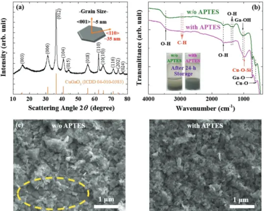
In order to prepare the metal-oxide HTL with a high coverage, controlling the nanoparticle size is important. We have used P123 as a surfactant in the hydrothermal synthesis to reduce the CuGaO2 particle size below 100 nm. X-ray diffraction (XRD) from the synthesized CuGaO2 nanoparticles exhibits peaks corresponding to CuGaO2 without impurity phases, confirming high purity of the CuGaO2 nanoparticles (Figure 1a). The grain size is ≈5 nm along the 〈001〉 direction and ≈35 nm for the 〈110〉 direction, as calculated by the Scherrer equation sug-gesting plate-shaped nanoparticles. To enhance the dispersion property of the nanoparticles in a solvent, APTES treatment is conducted (details in the Experimental Section). During the APTES treatment, hydroxyl groups on the nanoparticle surface are replaced by the silane groups of APTES, and the amine groups are exposed causing repulsive force between the nanoparticles, therefore enhancing their dispersion. The comparison of Fourier transform infrared (FTIR) spectra from CuGaO2 nanoparticles before and after the APTES treatment reveals that Cu–O–Si vibration peak (980 cm−1) appears after the APTES treatment with the disappearance of –OH groups
Figure 1. The effect of APTES treatment on the CuGaO2-nanoparticle nanostructures. a) X-ray diffraction of CuGaO2 nanoparticles, and extracted grain
size by Scherrer equation. b) FTIR of CuGaO2 nanoparticles. The inset shows optical images of nanoparticle suspension after 24 h storage with and w/o
(1337 and 1387 cm−1), as shown in Figure 1b.[31,38–40] This confirms that APTES becomes chemically adsorbed on the CuGaO2 nanoparticles via the silane group. It is noted that the vibrational modes of P123 surfactant used in the hydrothermal process are not observed confirming the complete removal of P123 after the washing step.
Even after storage for 24 h without stirring under ambient air, CuGaO2 nanoparticles in isopropyl alcohol (IPA) maintain their dispersion with APTES treatment (inset of Figure 1b). CuGaO2 film is deposited on the perovskite by spin-coating (Figure 1c). Without the APTES treatment, a low-coverage CuGaO2 film is resulted exposing some areas of the under-lying perovskite film (yellow circle). On the other hand, a full coverage film is obtained with the APTES-treated CuGaO2 nanoparticles. Although the APTES treatment enhances the dispersion of nanoparticles in suspension, careful adjustment of the treatment time is necessary so that the formation of multilayer APTES can be avoided: Otherwise, electrical conduc-tivity can decrease. The optimal treatment time is determined by in-plane conductivity measurements (Figure S1, Supporting Information).
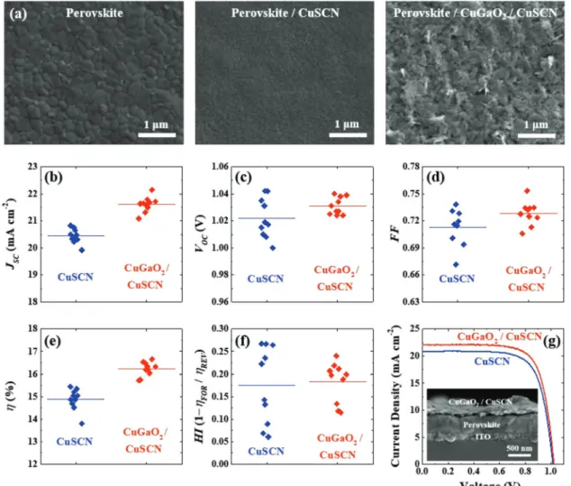
Solar cells comprised of SnO2 as an electron-transport layer, triple-cation perovskite [Cs0.05(FA0.83MA0.17)0.95Pb(I0.83Br0.17)3] as a light absorber, and either CuSCN or CuGaO2 with CuSCN (CuGaO2/CuSCN) as HTLs are fabricated (Figure 2a). The CuGaO2/CuSCN HTL is prepared by spin-coating CuGaO2 suspension, followed by spin-coating CuSCN solution. The schematic configuration of the solar cell with the expected energy-level diagram for each component is shown in Figure S2 (Supporting Information).[30,35,41–43] The photogenerated elec-trons in the perovskite absorber can be transferred to the SnO2 electron-transport layer, whereas holes can be transferred to the CuGaO2 or CuSCN. The holes injected into the CuGaO2 can be further transferred to the CuSCN, considering the energy-level diagram. As shown in Figure S3 (Supporting Information), the surface topography varies significantly depending on the types of HTLs. The root-mean-squared (RMS) roughness of the perovskite is 17.8 nm, and it is reduced to 7.4 nm after the deposition of CuSCN. For the CuGaO2-only HTL on perovskite, the RMS roughness exhibits the highest value of 40.9 nm, and it is reduced to 31.4 nm for the CuGaO2/CuSCN device, indi-cating that the CuSCN solution can infiltrate into a porous
Figure 2. Device performance without and with nanoparticles for the HTL. a) Morphologies of perovskite, perovskite/CuSCN, and perovskite/CuGaO2/
CuSCN by SEM. b) JSC, c) VOC, d) FF, e) η, and f) HI = 1 − ηFOR/ηREV of solar cells with different hole-transport layers. g) J–V curves of champion cells
CuGaO2 film reducing pinholes and roughnesses. The in-plane conductivity of the CuGaO2 film is not improved by the infil-trated CuSCN because the conductivity of the bare CuSCN is lower by more than an order of magnitude compared to the CuGaO2 film (Figure S4, Supporting Information). The average performance of solar cells with CuGaO2/CuSCN HTL improves compared to the CuSCN-only HTL (Figure 2b–f and Table 1). Photocurrent–voltage (J–V) curves of the best-performing cells are shown in Figure 2g (improved PCE of 16.7% from 15.4%). Shown in the inset of Figure 2g is a cross-sectional scan-ning electron microscope (SEM) image of the solar cell with the CuGaO2/CuSCN HTL which suggests a uniform layer of CuGaO2 infiltrated with CuSCN, instead of distinct bilayers of separate CuGaO2 and CuSCN. The optimum thicknesses of CuSCN-only and CuGaO2/CuSCN HTL are ≈90 and ≈170 nm, respectively (Figures S5 and S6, Supporting Information). The standard deviation of PCE for each device is less than 0.4% exhibiting outstanding reproducibility of our optimal devices (Table 1). As shown in Figure 2f, both devices using CuSCN-only or CuGaO2/CuSCN HTL exhibit similar average hysteresis indices (HI = 1 − ηFOR/ηREV). The main parameters affecting the hysteresis are VOC and FF for both devices (Figure S7, Sup-porting Information). The analogous behavior of the devices suggests that the properties of bulk perovskite and/or n-type electrode rather than those of the perovskite/HTL interfaces may dominantly affect the hysteresis, and detailed study of the cause of hysteresis is necessary as a future work. It is noted that PCE of a solar cell with CuGaO2-only HTL is lower than 4% due to the limited contact area between perovskite and CuGaO2 nanoparticles, causing potential shunting path from pinholes in the CuGaO2 layer (Figure S1, Supporting Information).[44]
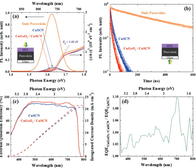
To better understand the reasons of the performance enhancement with the CuGaO2/CuSCN HTL, photolumines-cence (PL) analysis is carried out. For steady-state PL meas-urements, the excitation light is incident on the HTL side to probe the perovskite/HTL interface better. The PL intensity of the perovskite is substantially quenched with the presence of a HTL. However, the degree of the quench is larger for the CuGaO2/CuSCN compared to the CuSCN-only one (Figure 3a). It is noted that the PL peak position of the perovskite is close to the estimated optical bandgap (1.63 eV), that is, very small Stokes shift, suggesting the high quality of perovskite film,[45] and the blueshifted PL after the deposition of HTL suggests that additional defects are not generated at the perovskite/HTL interface.
The efficacy of carrier extraction across the perovskite/HTL is examined by time-resolved PL spectra (Figure 3b). Unlike the steady-state PL measurements, the excitation light is incident on the glass side to simulate the illumination condition iden-tical to the solar-cell operation. The PL lifetimes are ≈291, 17,
and 10 ns, respectively, for glass/perovskite, glass/perovskite/ CuSCN, and glass/perovskite/CuGaO2/CuSCN.[46] The reduced PL lifetime can be attributed to the efficient hole extraction from the perovskite to the HTL. When only CuGaO2 is used for the HTL, carrier extraction is less efficient compared to the CuGaO2/CuSCN owing to the insufficient contact area between the perovskite and the CuGaO2 (Figure S8, Supporting Infor-mation). The better hole extraction for the CuGaO2/CuSCN HTL compared to the only CuSCN or CuGaO2 HTL suggests that the infiltrated CuSCN into the porous CuGaO2 nanopar-ticle film enhances hole transfer from the perovskite. More efficient charge extraction between the perovskite and CuGaO2/ CuSCN HTL can also be inferred by the improved external quantum efficiency (EQE) response over the nearly entire wave-length range in which the solar cells respond (Figure 3c). Addi-tionally, the plot for the ratio of EQECuGaO2/CuSCN to EQECuSCN shows better EQE response at longer wavelength with the CuGaO2/CuSCN device, indicating improved hole carrier col-lection (Figure 3d).
Capacitance measurements of solar cells using two different HTLs exhibit a similar high-frequency plateau but dif-ferent response in a low-frequency range (Figure 4a). The high-frequency value can be attributed to the geometric/depletion capacitances, while the disparity in the low-frequency range can be ascribed to the difference in the trap density at the perovskite and/or interfaces.[42,47,48] The trap density can be estimated using the derivative of the capacitance with respect to the fre-quency, and the corresponding trap level with respect to the bandedge is related to the applied angular frequency.[42,47,48] The resultant distributions of trap density exhibit lower inte-grated trap density (by a Gaussian fitting) for the CuGaO2/ CuSCN device compared to the CuSCN-only device (Figure 4b). Therefore, it is deduced that wetting by CuSCN through the CuGaO2 nanoparticles may suppress or passivate surface/inter-face trap states.
The stability of a perovskite solar cell is evaluated under 85 °C/85% RH environment (Figure 4c). A much improved thermal stability is confirmed with the CuGaO2/CuSCN HTL: almost 80% of the initial PCE retention after 400 h. To inves-tigate the effect of CuGaO2 layer on the degradation between perovskite and CuSCN, perovskite films with each HTL (encapsulated by using poly(methyl methacrylate) (PMMA)) before and after storage at 85 °C for 100 h are analyzed by XRD (Figure S9, Supporting Information). We have compared the integrated-intensity ratios of a pristine sample to a sample after storage at 85 °C for 100 h for the perovskite and PbI2 peaks. The decomposition of perovskite and the formation of PbI2 are accelerated with the CuSCN compared to the bare perovskite film. The interfacial reaction between perovskite and CuSCN may aggravate the device stability at high temperature.[34] The Table 1. Photovoltaic parameters of the solar cells (reverse scans for ten cells). Devices without and with CuGaO2 nanoparticles for the HTL. The
data in the parentheses are from the highest efficient devices. HI, ηFOR, and ηREV are the hysteresis index, average photovoltaic efficiencies at forward
and reverse scans, respectively.
Sample Jsc [mA cm−2] Voc [V] FF η [%] HI [1−ηFOR/ηREV]
CuSCN 20.4 ± 0.3 (20.8) 1.02 ± 0.01 (1.02) 0.71 ± 0.02 (0.73) 14.9 ± 0.4 (15.4) 0.18 CuGaO2/CuSCN 21.6 ± 0.3 (22.1) 1.03 ± 0.01 (1.02) 0.73 ± 0.01 (0.74) 16.2 ± 0.3 (16.7) 0.18
degradation is mitigated by using CuGaO2 with CuSCN, which can be ascribed to the reduced contact area between perovskite and CuSCN.
Recently, Seok and co-workers have reported thermal sta-bility of CuSCN-based perovskite solar cells, and the efficiency
of their device rapidly degraded to ≈60% of the initial value (η = 18%) during the first 2 h at 125 °C.[49] Grätzel and co-workers have reported PCE exceeding 20% and the operational stability retaining ≈95% of initial value at 60 °C under illumina-tion for 1000 h.[24] Although our devices show lower PCE than Figure 3. Carrier extraction properties. a) Steady-state PL spectra (excitation wavelength = 532 nm) and plots of (αhυ)2 versus hυ for the
esti-mation of optical bandgap (Eg) of perovskite before/after the deposition of HTL. b) Time-resolved PL spectra with solid fitting lines (excitation
wavelength = 405 nm). c) External quantum efficiencies (EQEs) of the solar cells. d) The ratio of EQECuGaO2/CuSCN to EQECuSCN as a function of
wavelength.
Figure 4. Trap density analysis and stability of the devices. a) Frequency-dependent capacitances. b) Trap density of states as a function of trap level
with respect to the bandedge. The dashed lines denote Gaussian fitting for the trap density per volume (nt). c) Stability test of solar cells in 85 °C/85%
the reported values, we have shown that the interfacial p-type oxide layer can improve thermal stability by reducing the degra-dation reactions between the perovskite and CuSCN. Our find-ings emphasize that the mitigation of interfacial degradation is a key to improve the thermal stability of the perovskite solar cells.
3. Conclusions
We have fabricated perovskite solar cells with inorganic HTL consisting of CuGaO2 nanoparticle film and CuSCN to improve the thermal stability of devices. First, the dispersion of CuGaO2 nanoparticles in the suspension is enhanced by the surface modification of nanoparticles with aminosilane groups by APTES. After treatment, the resultant CuGaO2 suspension is effectively spin-coated yielding films with better coverage and uniformity. The HTL with a dual-inorganic layer CuGaO2/ CuSCN shows more efficient carrier extraction from the under-lying perovskite. This leads to the improved EQE response, and therefore, a higher short-circuit current from the CuGaO2/ CuSCN solar cell. The trap density is also reduced by ≈40% by the CuGaO2/CuSCN compared to the CuSCN-only case. Con-sequently, the average PCE for the CuGaO2/CuSCN solar cells is larger than the CuSCN-only solar cells. The encapsulated CuGaO2/CuSCN solar cell maintains ≈80% of its initial PCE for 400 h under 85 °C/85% RH condition. Our study presents an effective strategy that can both improve performance and thermal stability of perovskite solar cells.
4. Experimental Section
Synthesis of CuGaO2 Nanoparticles and APTES Treatment: 7 g of
P123 (Sigma-Aldrich) was dissolved in 140 mL of deionized (DI) water by stirring for 4 h at room temperature (RT). Then 2 mmol of Cu(NO3)2·2.5H2O (Alfa Aesar) and Ga(NO3)3·xH2O (Alfa Aesar), 4 mL
of ethylene glycol (Alfa Aesar), and 4.5 mL of 1 m KOH aqueous solution
(Daejung) were added sequentially during vigorous stirring. After the solution was stirred for 1 h, the precursor was transferred to 200 mL Teflon-lined stainless-steel autoclave. The sealed autoclave was placed in a preheated oven at 220 °C for 4 h, then cooled under water flow. The synthesized particles were centrifuged and washed with diluted ammonia solution (5 wt%), diluted nitric acid (5 wt%), and DI water for two times, respectively. Then, the particles were additionally washed with ethyl alcohol for three times and isopropyl alcohol (IPA) for five times. For surface modification, 1 vol% of APTES (Sigma-Aldrich) was added to the CuGaO2 suspension in IPA (10 mg mL−1), and stirred for 3 h
at 30 °C. After the reaction, the suspension was ultrasonically treated for 2 min, and washed with IPA for three times to remove any physically adsorbed APTES.
Device Fabrication: Indium tin oxide (ITO) glasses were ultrasonically
cleaned in acetone, ethanol, and deionized water, followed by a UV–ozone treatment for 15 min. For SnO2 electron-transport layer,
15 wt% SnO2 aqueous solution (Alfa Aesar) was diluted in DI water with
the volume ratio of 1:4. The solution was spin-coated at 3000 rpm for 30 s, and annealed at 120 °C for 30 min. The 1.3 m precursor solution
for the Cs0.05(FA0.83MA0.17)0.95Pb(I0.83Br0.17)3 perovskite was prepared by
dissolving cesium iodide (CsI, TCI Chemicals), formamidinium iodide (FAI, Greatcell Solar), methylammonium bromide (MABr, Greatcell Solar), lead iodide (PbI2, TCI Chemicals), and lead bromide (PbBr2,
TCI Chemicals) in a mixture of N,N-dimethylformamide (DMF, Sigma-Aldrich) and dimethyl sulfoxide (DMSO, Sigma-Sigma-Aldrich) with the volume
ratio of 4:1. The solution was deposited onto the substrate by spin-coating at 5000 rpm for 20 s, and 300 µL of chlorobenzene was dripped at 17 s during the spinning process. Then, the film was annealed at 100 °C for 45 min. For the CuGaO2 hole-transport layers, CuGaO2 suspension
in IPA (20 mg mL−1) was used for spin-coating at 3000 rpm for 30 s. The
spin-coating was conducted for two times, then the film was annealed at 100 °C for 5 min. To deposit CuSCN film (for both CuSCN-only and CuGaO2/CuSCN), CuSCN solution in diethyl sulfide (24 mg mL−1) was
used for spin-coating at 3000 rpm for 30 s, and annealed at 50 °C for 10 min. Finally, 150-nm-thick Au electrodes were deposited by thermal evaporation. For the stability test, devices were encapsulated using cover glass with UV-curable epoxy resin in a glovebox.
Characterization: The crystal structure and grain size of CuGaO2
nanoparticles were analyzed by XRD (D8 Advance: Bruker). FTIR spectroscopy (TENSOR27: Bruker) was carried out to observe vibrational modes of chemical bonding in CuGaO2 nanoparticles. The
morphologies of the films were observed using a field-emission scanning electron microscope (FESEM, Merlin-Compact: Carl Zeiss). The surface topography of the film was obtained by atomic force microscopy (NX-10: Park Systems). The absorbance was obtained by a UV–vis spectrophotometer (V-770: JASCO). Steady-state and time-resolved photoluminescence spectra were observed in the films prepared on glass substrates with excitation wavelength of 532 and 405 nm (LabRAM HV Evolution: Horiba, FluoTime 300: Picoquant), respectively. The photocurrent–voltage (J–V) curves of the solar cells were measured using a solar cell measurement system (K3000: McScience, AM 1.5G, 100 mW cm−2), with an active area of 0.09 cm2 and 100 mV s−1 voltage
scan rate. The EQE spectra were obtained by an incident photon-to-current conversion efficiency (IPCE) measurement system (K3100: McScience). Frequency-dependent capacitances were obtained by impedance analysis in dark condition using a potentiostat (Zive SP1: WonATech Co., Ltd.) with 50 mV amplitude of ac signal at zero applied bias and frequency ranging from 0.01 to 105 Hz.
Supporting Information
Supporting Information is available from the Wiley Online Library or from the author.
Acknowledgements
This work was supported by the Korea Institute of Energy Technology Evaluation and Planning (KETEP: 20183010014470).
Conflict of Interest
The authors declare no conflict of interest.
Keywords
CuGaO2, CuSCN, long-term stability, perovskite solar cells
Received: August 7, 2019 Revised: September 1, 2019 Published online:
[1] A. Polman, M. Knight, E. C. Garnett, B. Ehrler, W. C. Sinke, Science
2016, 352, aad4424.
[2] N. J. Jeon, H. Na, E. H. Jung, T.-Y. Yang, Y. G. Lee, G. Kim, H.-W. Shin, S. I. Seok, J. Lee, J. Seo, Nat. Energy 2018, 3, 682.
[3] R. Saive, M. Boccard, T. Saenz, S. Yalamanchili, C. R. Bukowsky, P. Jahelka, Z. J. Yu, J. Shi, Z. Holmanb, H. A. Atwater, Sustainable
Energy Fuels 2017, 1, 593.
[4] S. Lee, J. C. Flanagan, J. Kim, A. J. Yun, B. Lee, M. Shim, B. Park,
ACS Appl. Mater. Interfaces 2019, 11, 19104.
[5] H. H. Park, R. Heasley, L. Sun, V. Steinmann, R. Jaramillo, K. Hartman, R. Chakraborty, P. Sinsermsuksakul, D. Chua, T. Buonassisi, R. G. Gordon, Prog. Photovoltaics 2015, 23, 901. [6] T. Hwang, D. Cho, J. Kim, J. Kim, S. Lee, B. Lee, K. H. Kim, S. Hong,
C. Kim, B. Park, Nano Energy 2016, 25, 91.
[7] J. Kim, T. Hwang, B. Lee, S. Lee, K. Park, H. H. Park, B. Park, Small
Methods 2019, 3, 1800361.
[8] J. Kim, A. J. Yun, B. Gil, Y. Lee, B. Park, Adv. Funct. Mater. 2019, https://doi.org/10.1002/adfm.201905190.
[9] T. Hwang, B. Lee, J. Kim, S. Lee, B. Gil, A. J. Yun, B. Park, Adv. Mater.
2018, 30, 1704208.
[10] B. Lee, B. Shin, B. Park, Electron. Mater. Lett. 2019, 15, 192. [11] Q. Wang, B. Chen, Y. Liu, Y. Deng, Y. Bai, Q. Dong, J. Huang,
Energy Environ. Sci. 2017, 10, 516.
[12] N. Aristidou, C. Eames, I. Sanchez-Molina, X. Bu, J. Kosco, M. S. Islam, S. A. Haque, Nat. Commun. 2017, 8, 15218.
[13] N. Aristidou, I. Sanchez-Molina, T. Chotchuangchutchaval, M. Brown, L. Martinez, T. Rath, S. A. Haque, Angew. Chem., Int. Ed.
2015, 54, 8208.
[14] J. H. Noh, S. H. Im, J. H. Heo, T. N. Mandal, S. I. Seok, Nano Lett.
2013, 13, 1764.
[15] M. Saliba, T. Matsui, J.-Y. Seo, K. Domanski, J.-P. Correa-Baena, M. K. Nazeeruddin, S. M. Zakeeruddin, W. Tress, A. Abate, A. Hagfeldt, M. Grätzel, Energy Environ. Sci. 2016, 9, 1989.
[16] T. Matsui, T. Yamamoto, T. Nishihara, R. Morisawa, T. Yokoyama, T. Sekiguchi, T. Negami, Adv. Mater. 2019, 31, 1806823.
[17] J. Kim, T. Hwang, S. Lee, B. Lee, J. Kim, G. S. Jang, S. Nam, B. Park,
Sci. Rep. 2016, 6, 25648.
[18] T. Leijtens, K. Bush, R. Cheacharoen, R. Beal, A. Bowring, M. D. McGehee, J. Mater. Chem. A 2017, 5, 11483.
[19] A. K. Jena, M. Ikegami, T. Miyasaka, ACS Energy Lett. 2017, 2, 1760. [20] A. K. Jena, Y. Numata, M. Ikegami, T. Miyasaka, J. Mater. Chem. A
2018, 6, 2219.
[21] J. Zhang, T. Zhang, L. Jiang, U. Bach, Y.-B. Cheng, ACS Energy Lett.
2018, 3, 1677.
[22] N. Li, S. Tao, Y. Chen, X. Niu, C. K. Onwudinanti, C. Hu, Z. Qiu, Z. Xu, G. Zheng, L. Wang, Y. Zhang, L. Li, H. Liu, Y. Lun, J. Hong, X. Wang, Y. Liu, H. Xie, Y. Gao, Y. Bai, S. Yang, G. Brocks, Q. Chen, H. Zhou, Nat. Energy 2019, 4, 408.
[23] Z. Yu, L. Sun, Small Methods 2018, 2, 1700280.
[24] N. Arora, M. I. Dar, A. Hinderhofer, N. Pellet, F. Schreiber, S. M. Zakeeruddin, M. Grätzel, Science 2017, 358, 768.
[25] I. S. Yang, S. Lee, J. Choi, M. T. Jung, J. Kim, W. I. Lee, J. Mater.
Chem. A 2019, 7, 6028.
[26] Q. Wu, C. Xue, Y. Li, P. Zhou, W. Liu, J. Zhu, S. Dai, C. Zhu, S. Yang,
ACS Appl. Mater. Interfaces 2015, 7, 28466.
[27] P. Nazari, F. Ansari, B. A. Nejand, V. Ahmadi, M. Payandeh, M. Salavati-Niasari, J. Phys. Chem. C 2017, 121, 21935.
[28] Y. Yang, H. Chen, X. Zheng, X. Meng, T. Zhang, C. Hu, Y. Bai, S. Xiao, S. Yang, Nano Energy 2017, 42, 322.
[29] S. Akin, Y. Liu, M. I. Dar, S. M. Zakeeruddin, M. Grätzel, S. Turan, S. Sonmezoglu, J. Mater. Chem. A 2018, 6, 20327.
[30] S. S. Mali, J. V. Patil, H. Kim, R. Luque, C. K. Hong, Mater. Today
2019, 26, 8.
[31] C. Liu, X. Zhou, S. Chen, X. Zhao, S. Dai, B. Xu, Adv. Sci. 2019, 6, 1801169.
[32] J. W. Jo, Y. Yoo, T. Jeong, S. J. Ahn, M. J. Ko, Electron. Mater. Lett.
2018, 14, 657.
[33] B. Gil, A. J. Yun, Y. Lee, J. Kim, B. Lee, B. Park, Electron. Mater. Lett.
2019, 15, 505.
[34] J. Liu, S. K. Pathak, N. Sakai, R. Sheng, S. Bai, Z. Wang, H. J. Snaith,
Adv. Mater. Interfaces 2016, 3, 1600571.
[35] H. Zhang, H. Wang, W. Chen, A. K.-Y. Jen, Adv. Mater. 2017, 29, 1604984.
[36] R.-S. Yu, Y.-C. Lee, Thin Solid Films 2018, 646, 143.
[37] K. Ueda, T. Hase, H. Yanagi, H. Kawazoe, H. Hosono, H. Ohta, M. Orita, M. Hirano, J. Appl. Phys. 2001, 89, 1790.
[38] R. G. Kadam, A. K. Rathi, K. Cepe, R. Zboril, R. S. Varma, M. B. Gawande, R. V. Jayaram, ChemPlusChem 2017, 82, 467. [39] D. P. Sahoo, S. Patnaik, D. Rath, B. Nanda, K. Parida, RSC Adv.
2016, 6, 112602.
[40] M. Selvaraj, B. H. Kim, T. G. Lee, Chem. Lett. 2005, 34, 1290. [41] K. Sugiyama, H. Ishii, Y. Ouchi, K. Seki, J. Appl. Phys. 2000, 87, 295. [42] A. J. Yun, J. Kim, T. Hwang, B. Park, ACS Appl. Energy Mater. 2019,
2, 3554.
[43] J. Tirado, C. Roldán-Carmona, F. A. Muñoz-Guerrero, G. Bonilla-Arboleda, M. Ralaiarisoa, G. Grancini, V. I. E. Queloz, N. Koch, M. K. Nazeeruddin, F. Jaramillo, Appl. Surf. Sci. 2019, 478, 607.
[44] V. Tunuguntla, W.-C. Chen, T. D. Newman, C.-Y. Chen, M.-C. Hsieh, S.-H. Lu, C. Su, L.-C. Chen, K.-H. Chen, Sol. Energy Mater. Sol. Cells
2016, 149, 49.
[45] H. Tsai, W. Nie, J.-C. Blancon, C. C. Stoumpos, R. Asadpour, B. Harutyunyan, A. J. Neukirch, R. Verduzco, J. J. Crochet, S. Tretiak, L. Pedesseau, J. Even, M. A. Alam, G. Gupta, J. Lou, P. M. Ajayan, M. J. Bedzyk, M. G. Kanatzidis, A. D. Mohite, Nature 2016, 536, 312. [46] J. I. Kim, J. Kim, J. Lee, D.-R. Jung, H. Kim, H. Choi, S. Lee, S. Byun,
S. Kang, B. Park, Nanoscale Res. Lett. 2012, 7, 482.
[47] T. Hwang, A. J. Yun, J. Kim, D. Cho, S. Kim, S. Hong, B. Park,
ACS Appl. Mater. Interfaces 2019, 11, 6907.
[48] B. Lee, T. Hwang, S. Lee, B. Shin, B. Park, Sci. Rep. 2019, 9, 4803. [49] M. Jung, Y. C. Kim, N. J. Jeon, W. S. Yang, J. Seo, J. H. Noh,