High-Frequency Dimmable Electronic Ballast for Automotive HID Lamps
Huang-Jen Chiu1,Hsiu-Ming Huang1, Li-Wei Lin1 1Dept. of Electrical Engineering,
Chung-Yuan Christian Univ., Taiwan
Shann-Chyi Mou2
2Dept. of Mechanical Engineering,
Ching-Yun Univ., Taiwan
Pang-Jung Liu3
3Elan Microelectronics Corporation,
Taiwan
Abstract— This paper presents a high-frequency
electronic ballast for HID lamps. A new fixed frequency dimming method with low EMI features is developed in this research. The proposed electronic ballast has the advantages of high power density, simple circuit and low EMI features. The circuit operating principle and design procedures are described in detail. A laboratory prototype was built and tested. The simulation and experimental waveforms verify the feasibility of the proposed scheme. Keywords⎯ High-Frequency Dimmable Electronic Ballast, HID Lamp, Soft Switching
I. Introduction
Because of their much higher luminous efficacy, better color rendition, and longer lifetime than fluorescent lamps, High Intensity Discharge (HID) lamps have been used in various commercial and industrial applications such as street lighting, LCD projectors, and automotive headlights. Like fluorescent lamps, the HID lamp exhibits the negative impedance characteristic, and thus needs an auxiliary circuit namely “a ballast” to ensure stable lamp operation. The conventional magnetic ballast is bulky, heavy, and does not easily to dim the lamp. The electronic ballast, based on solid-state devices, can overcome most of the drawbacks in the magnetic ballast. However, periodic HID lamp excitation at the 10kHz to 300kHz frequency range can lead to acoustic resonance that produces an unstable arc and even cracks the tube. Some electronic ballasts operate the lamp with a low-frequency (50-400Hz) square-wave To avoid this acoustic resonance. [1-3]. A conventional electronic ballast for driving HID lamps consisted of a front-end DC/DC converter and a low-frequency DC/AC inverter, as shown in Figure 1. The front-end DC/DC converter is usually a Flyback converter that draws power from a low-voltage source (i.e. battery or fuel cell) and feeds a high-voltage DC bus for the post-stage DC/AC inverter. The DC/AC inverter is operated at low frequency to avoid acoustic resonance. The low-frequency electronic ballast is therefore still large and heavy as the magnetic ballast. This paper presents a single-stage electronic ballast that provides high-frequency power to HID lamps without acoustic resonance. The high-frequency electronic ballast produces an increase in lamp illumination in an improved compact, light weight package. The switching frequency or duty ratio of the solid-state devices in the electronic ballast can be varied to dim the lamp [4-7]. The dimming range is usually too narrow to adopt the duty ratio regulation method. Varying the electronic ballast switching frequency produces a wide dimming range. However, switching frequency variations cause difficulty in magnetic component design and electromagnetic interference (EMI) suppression. A fixed switching frequency dimming method is proposed to achieve better
EMI features. In the following sections, the circuit configuration and characteristic analysis will be addressed in detail. The simulation and experimental results from a laboratory prototype are presented to show the feasibility of the proposed scheme.
Fig. 1 A Conventional Configuration of the Electronic Ballast for HID Lamps
II. Electronic Ballast Circuit and Dimming Operation
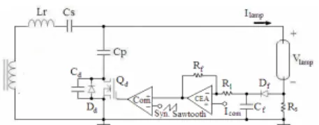
Figure 2 shows the proposed high frequency dimmable electronic ballast for driving HID lamps. This ballast consists of a phase-shifted full-bridge inverter, a boost transformer, a resonant tank and a dimming circuit. Both power switch pairs Q1, Q3 and Q2, Q4 are operated at a fixed switching frequency. By varying the phase shift between the switch pairs, a quasi-square wave PWM voltage will be produced across the transformer primary winding. The boost transformer provides the desired high level quasi-square voltage on the secondary winding and offers isolation between the low- and high-voltage sides for safety purposes. A series-resonant parallel-loaded (SRPL) circuit is adopted to satisfy the starting and steady HID lamp characteristics. To achieve wider HID lamp dimming range, a dimming circuit is added, as shown in Figure 2. The proposed dimming method adopts a switched-capacitor controller that regulates the SRPL circuit resonance frequency to dim the HID lamp. This method retains low EMI fixed switching frequency features for the electronic ballast while providing good dimming control. Figures 3(a) and (b) show the topology and waveforms of the full-wave switched-capacitor dimming circuit. A sinusoidal current IAB flows from
terminal A to terminal B. The gating signals for the dimming switches, Qd1 and Qd2 are synchronized with
current IAB. They exhibit a phase shift φ from IAB and
complement each other. Switches Qd1 and Qd2 are
zero-voltage turned on and off. The switching losses of the dimming switches are minimized. Figures 3(c) and (d) show the topology and waveforms for another dimming circuit with a half-wave switched-capacitor. The positive IAB current flows through the dimming switch Qd while
the negative current flows through the anti-paralleled diode Dd. The dimming switch, Qd is turned on and off
with ZVS features. The equivalent dimming capacitance Cd(eq) can be derived as follows [8].
π φ − φ − = k / ) 2 sin 2 ( 2 C Cd(eq) d , (1)
where, k is 1 or 2 for full- and half-wave switched-capacitor circuits, respectively. The equivalent dimming capacitance Cd(eq) can be modulated by changing
the phase shift φ. The switched-capacitor control technique can be used to vary the resonant frequency of the load resonant circuit. In other words, the phase shift φ of the dimming switches can be used as a control parameter to vary the lamp power.
Fig. 2 The Proposed Dimmable Electronic Ballast for HID Lamps
III. Design Considerations
A. Resonant Inverter
The quasi-square wave voltage Vab supplied by the
phase-shifted full bridge inverter and boost transformer is applied to the HID lamp through the load resonant circuit. Using Fourier analysis, Vab can be expressed as follows.
)] t f 2 sin( ) 2 n cos( ) n V 4 [( V s 5 , 3 , 1 n P ab = ∑ π α π ∞ = , (2)
where, VP, fs and α are the peak value, switching
frequency and phase shift of the PWM voltage on the transformer secondary winding. Assuming load quality factor Q for the resonant tank at the resonant frequency, fo
is high enough, only the fundamental component V1 of
Vab will be present in the load resonant circuit. The lamp
voltage Vlamp(rms) can be derived as follows.
2 s o o s 2 2 o s 2 ) rms ( 1 ) rms ( amp 1 )] 1 f f f f ( Q 1 [ ] ) f f ( 1 [ ) 1 ( V V Ω + Ω − + − Ω + = , (3) where the root mean square value, V1(rms) of V1, the
resonant frequency, fo and load quality factor, Q at the
resonant frequency can be expressed as follows.
) 2 cos( V 2 2 V1(rms) = π P α , (4) r r o C L 2 1 f π = , (5) r r lamp o lamp C L / R Z R Q= = , (6) s ) eq ( p C C = Ω , (7) ) eq ( d p ) eq ( d p ) eq ( p C C C C C + = , (8) where Cr is the total resonant capacitance that includes the
series capacitor, Cs, paralleled capacitor, Cp and
equivalent dimming capacitance, Cd(eq) and can be
represented as follows. ) eq ( p s ) eq ( p s r C C C C C + = , (9)
The resonant current, ILr(rms) can then be expressed
as Equation (10). Based on Equation (3), the lamp power can be derived as Equation (11).
) 1 f f f f ( Q 1 j ] ) f f ( 1 )[ 1 ( ) 1 ( f f jQ 1 ) 2 cos( V 2 2 I s o o s 2 o s o s P ) rms ( Lr Ω + Ω − + − Ω + Ω + + π α = , (10) 2 s o o s 2 2 o s 2 2 lamp 2 2 P lamp 2 ) rms ( lamp lamp )] 1 f f f f ( Q 1 [ ] ) f f ( 1 [ ) 1 ( ) 2 ( cos R V 8 R V P Ω + Ω − + − Ω + α π = = , (11) During the dimming operation, the HID lamp can be
modeled using negative resistance characteristics developed as follows. lamp H S lamp lamp lamp I R IV V R = = + , (12)
where VH and RS are the two characteristic parameters of
the modeled HID lamp. The dimming capacitance Cd is
modulated to vary the resonant frequency of the load resonant circuit. In other words, the phase shift φ of the dimming switches can be used as a control parameter to vary the lamp power.
The voltage and current ratings for the power switches are important inverter design issues. Low rating switches are allowed for the used full-bridge topology. Another important point of concern is that a high Q value will provide higher calculations precision using the fundamental approach and a smaller resonant inductor. B. Ignition Considerations
Figure 2 shows how a pulse igniter can be implemented. A voltage doubler, a spark gap, and a pulse transformer must be added to the power circuit. Before the ignition, the HID lamp can be considered an open circuit. The voltage doubler boosts its output voltage to reach the breakdown voltage (2.4kV) of the spark gap. When the spark gap turns on, the pulse transformer induces a required high voltage (about 20kV) at its secondary winding to ignite the HID lamp. After ignition, a warm-up current of 500%-700% of the nominal current is required [9].
C. Soft Switching Control
There are three different commutation modes given by the resonant current, ILr signs at θ=α and at θ=π [10].
In the forced commutation operation shown in Fig. 4(a), the power switches present zero-voltage-switching (ZVS). However, they are turned off with current and generate undesired turn-off losses. In the natural commutation operation shown in Fig. 4(b), the power switches can be operated with zero-current-switching (ZCS) features. However, they are turned on with voltage and generate turn-on losses. In the mixed commutation operation shown in Fig. 4(c), one of the legs presents ZVS and the other presents ZCS features. As shown in Fig. 4(d), the boundary between the forced and mixed commutation modes is considered the optimum operation point. In this
case, the switches, Q2 and Q4, are turned on and off at the resonant current zero crossing. All of the power switches present ZVS features and one of the legs presents ZCS features. A fixed-frequency phase-shifted PWM controller, shown in figure 5, is used in this study to achieve the optimum commutation. The gating signals for one of the legs (Q1, Q3) are generated by a fixed frequency square-wave oscillator. The zero-crossing point of the resonant current, ILr is detected to generate the gating
signals for the other leg (Q2, Q4). D. Dimming Circuit
The half-wave switched-capacitor is used to regulate the lamp power. The detailed schematic diagram of the proposed dimming circuit is depicted in Figure 6. The peak lamp current value, Ilamp is measured and compared
with a current command, Icom. The phase shift φ of the
dimming switch, Qd is modulated to regulate the lamp
power in according to the current error amplifier (CEA) output.
(a) (b)
(c) (d)
Fig. 3 (a) Topology and (b) Key Waveforms of Full-Wave Switched-Capacitor Dimming Circuit, and (c) Topology and (d) Key Waveforms of Half-Wave witched-Capacitor Dimming Circuit
(a) Forced Commutation (b) Natural Commutation
(c) Mixed Commutation (d) Optimum Commutation Fig. 4 Voltage and Current Waveforms for the Different Commutation Modes
Fig. 5 A Fixed-Frequency Phase-Shifted PWM Controller
Fig. 6 The Detailed Schematic Diagram of the Proposed Dimming Circuit
IV. Simplified Design Example
To verify the feasibility of the proposed electronic ballast, a laboratory prototype with following specifications was designed and tested for driving an OSRAM HID lamp HTIS35/12.
Source Voltage: 9~16V (Nominal Voltage 12V) Rated Power: 35W (Maximum Power 70W)
Lamp Data: Rated Voltage 85V, Rated Current 2.5A (max), Ignition Voltage 23kV (max)
The nominal voltage of the HID lamp was 85V, however, a maximum voltage of 100V is used in the dimming operation. While the rated power is 35W, the transient power during ignition is about 70W. The design procedure for the proposed ballast is summarized as follows:
1. Switching Frequency. To avoid acoustic resonance, the ballast could be designed to operate at a non-resonance frequency within a narrow medium-frequency band (typically in the range of 22 to 28kHz). However, it is not practical because this frequency depends on the lamp characteristics. This HID lamp high-frequency ballast ensures resonance-free operation by operating the lamp above the highest acoustic resonance, 300kHz. For EMI considerations, it might be desirable that the switching frequency stay below 450kHz. Therefore, the switching frequency of the proposed ballast is designed at 430kHz.
2. Phase shift α value selection. This parameter affects the lamp power. To operate with nominal lamp power, we must choose the α= 0.
3. Ω parameter selection. A large Ω produces a small Cs and large Lr. On the other hand, a small Ω produces a
large Cs and small Lr and more harmonics in the lamp
current. The appropriate value was chosen as Ω=1. 4. Transformer turn ratio, n. A boost transformer is necessary to provide the desired high level for quasi-square voltage on its secondary winding and offers isolation between the low- and high-voltage sides for safety purpose. For the nominal battery voltage, VBat=12V
and the amplitude of the secondary winding voltage, Vp=120V, an adequate value was chosen n=10 (3:30).
5. Resonance frequency determination under rated power operation, fo(Rate). Figure 7 shows the characteristic
curve for Ω=1. For the nominal lamp voltage 85V, we can determine the resonance frequency, fo(Rate)=480kHz and
loaded quality factor, Q=0.4 under rated power operation. 6. HID lamp characteristic resistance calculation under rated power operation, Rlamp(Rate). The two
parameters, VH and Rs can be determined from the
measured lamp data. The HID lamp characteristic resistance can then be calculated based on Equation (12). Rlamp(Rate)=212.5Ω.
7. Resonance parameters selection. Based on Equations (5) to (9), the resonant elements can be obtained as follows. 7 o r rC 21f 3.3 10 L = × − π = , (13) ) ( 25 . 531 Q / R C L lamp r r = = Ω , (14) r ) eq ( p s C 2C C 1⇒ = = = Ω , (15) ) C ( operation power rated for , C Cp(eq)= p d(eq)=∞,(16) Choose Lr=175µH, Cs= Cp=1.2nF.
8. Dimming capacitance, Cd selection. The phase shift
φ of the dimming switch, Qd is used as a control
parameter to vary the lamp power. For the rated power operation, the dimming switch is designed to operate with the phase shift φ=2π. Based on Equation (1), the equivalent dimming capacitance, Cd(eq) is ∞. For the
dimmest operation, the dimming switch should be designed to operate with a φ=0 phase shift. Therefore, the equivalent dimming capacitance, Cd(eq) is Cd/2. For the
maximum lamp voltage limit under the dimmest operation, the proper dimming capacitance, Cd can be determined. In
this laboratory prototype, the dimming capacitance, Cd is
chosen to equal to Cp for implementing convenience.
Fig. 7 The Design Curve for the Resonance Tank of the Proposed Ballast
V. Simulation and Experimental Verification
The circuit parameters for the design example previously shown in the last section are summarized in Table I. A laboratory prototype was built and tested using these circuit parameters. The simulation and experimental results are shown in Figures 8~11 to verify the feasibility of the proposed scheme. The lamp power is controlled from 100% to 30% of the rated power by adopting the proposed dimming technique. The Figure 8 shows the simulation and measured waveforms of Vds1 and Vgs1
illustrating the ZVS and ZCS feature for the power MOSFETs. Figure 9 shows the simulation and measured waveforms of Vab and ILr. Figure 10 shows the waveforms
for the lamp voltage Vlamp and current Ilamp of the
laboratory prototype operated at the rated power and a dimmest power of 30%, respectively. The efficiency variations in the design example for the dimming operation are shown in Fig. 11. High efficiency can be achieved.
(a) (b)
Fig. 8 (a) Simulation and (b) Measured Waveforms of Vds1 and Vgs1
(a) (b)
Fig. 9 (a) Simulation and (b) Measured Waveforms of Vab
and ILr
(a) Rated Power (b) Dimmest Power Fig. 10 Measured Waveforms for the Lamp Voltage, Vlamp
and Current, Ilamp
Fig. 11 The Efficiency Variations for the Dimming Operation
Table 1 The Component List for the Laboratory Prototype Component Description Symbol Value/Part no.
Power Switches Q1~Q4 IRFZ24N Power Transformer TR TDK EI22, Np=3T,
Ns=30T
Resonance Inductor Lr 175µH
Series Capacitor Cs 1.2nF
Parallel Capacitor Cp 1.2nF
Dimming Capacitor Cd 1.2nF
Dimming Switch Qd IRF840
VI. Conclusion
We presented an electronic ballast for driving HID lamps with high frequency operation. The fixed-frequency dimming technique is used to achieve wide dimming range. The proposed electronic ballast has the advantages of high power density, simple circuit and low EMI features. The detailed operating principles and design considerations for the proposed electronic ballast were described and analyzed. Laboratory prototype experimental results were shown to verify the feasibility of the proposed method. The results were satisfactory.
Acknowledgment
The authors would like to acknowledge the financial support from the National Science Council of Taiwan, R. O. C. through grant number NSC 93-2213-E-033-009.
References
[1] Kyu-Chan Lee; and Bo Hyung Cho, “Design and Analysis of Automotive High Intensity Discharge Lamp Ballast using Micro Controller Unit,” IEEE Transactions on Power Electronics, Vol. 18, pp. 1356-1364, Nov. 2003.
[2] Jinghai Zhou, Fengfeng Tao, Lee, F. C., Onishi, N., and Okawa, M., ”High Power Density Electronic Ballast for HID Lamps,” IEEE IAS’02, Vol. 3, pp. 1875-1880.
[3] Miaosen Shen, Zhaoming Qian, Fang Zheng Peng, “Design of a Two-Stage Low-Frequency Square-Wave Electronic Ballast for HID Lamps,” IEEE Transactions on Industry Applications, Vol.
39, pp. 424-430, March-April 2003.
[4] Xiaohong Cao, Wei Yan, Hui, S. Y., Chung, H. S. H., “Dimming Control and Characteristics of High-Frequency Operated Metal Halide Lamps,” IEEE Transactions on Power Electronics, Vol. 19, pp. 854-861, May 2004.
[5] Bor-Ren Lin, and Yuen-Chou Hsieh, “Dimming Control of Metal Halide Lamp with High Power Factor,” IEEE ISIE'99, Vol. 2, pp. 590-595.
[6] Ohsato, N. H., Ohguchi, H., Shimizu, T., Kimura, G., and Takagi, H. “New Type of Ballast for HID Lamps Using Distributed Constant Line,” PCC’97, Vol. 2, pp. 987-990.
[7] Co, M. A., Brumatti, M., Simonetti, D. S. L., and Vieira, J. L. F., ”Single Stage Electronic Ballast for HID Lamps,” IEEE IAS’03, Vol. 1, pp. 339-344. [8] W. J. Gu and K. Harada, “A New Method to
Regulate Resonant Converters,” IEEE Transactions on Power Electronics, Vol. 3, pp. 430 -439, Oct. 1988.
[9] Redl, R., and Paul, J. D., “A New High-Frequency and High-Efficiency Electronic Ballast for HID Lamps: Topology, Analysis, Design, and Experimental Results,” IEEE APEC'99, Vol. 1, pp. 486- 492.
[10] Alonso, J. M., Rico, M., Blanco, C., and Lopez, E., “A Novel Low-Loss Clamped-Mode LCC Resonant Inverter for HID Lamp Supply,” IEEE PESC'95, Vol. 2, pp. 736-742.