ICCAS2005 June 2-5, KINTEX, Gyeonggi-Do, Korea
1. INTRODUCTION
As we known the digital image processing system requires high speed and efficient processing unit to run in real-time systems. Traditional approach can be processed using PC with the high speed and performance such as mainframe. Therefore, the regular personal computer is not suitable if we want to work in real time system. At present, people prefer a small system which can process correctly and fast. Therefore, our research present a designing of wavelet transform through lifting scheme implementing on small FPGA system. The wavelet transform is widely used in signal processing. Moreover, wavelet transform can be applied in many applications [1, 2]. The accuracy of wavelet transform depends on the design of low and high pass filter, which represent the scaling function of the Mother wavelet. The results from scaling function is down-sampled[3]. The advantage of the proposed method is that it can process wavelet transformation of an image fast and efficient.
Typically, the image and digital signal processing applications require high calculation throughput [4, 5]. The arithmetic operators presented here are implemented for real time signal processing. We design floating-point arithmetic based on IEEE754 standard [6]. We designed 32-bit floating-point computation which is fine enough for image and digital signal processing application. After that, we arrange our floating-point arithmetic unit according to Daubechies4 transform though lifting scheme equation [7, 8]. All constants of equations are transformed to the format according to IEEE754 before processed to reduce complexity of the computation. The results of Daubechies4 equations consist of approximation and detail. In this module, we can use parallel processing properties of FPGA to calculate approximation and detail simultaneously.
2. OVERVIEW OF THE PROPOSED DWT
ARCHITECTURE ON FPGA
The overview structure of DWT is shown in Fig.1. First, this module receives 32-bit input which is already in IEEE754 standard format. Next, the input is processed with Daubechies4 equations within module. Internal structure of the module composes of floating-point units which can compute addition, subtraction andmultiplication according to the equations. The results are the coefficients of both low and high filters. We call the results as “approximation” and
“detail” respectively. The designing and internal structure will be described in next section.
Fig. 1 Internal structure of DWT 2.1 Floating Point Format Representation
The designing of real number computation module is referred to IEEE754 standard. We use 32 bit format as shown in Fig.2. “s” is sign bit, “c” is exponent field and “f” is mantissa field to collect floating-point. The value of each part can be calculated as shown in Eq. (1).
Fig. 2 32 Bit Floating Point Format. 2.2 Floating Addition and Subtraction
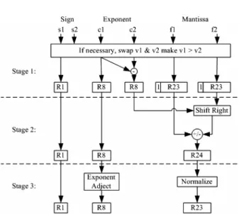
Most of addition and subtraction process of real number follows the same processing step to get the result. However, there are some different parts needed to be changed from minus to addition as shown in Fig. 4 in stage 2 above 24-bit register (R24). Fig.3 shows all fields of input data. V1 is the first input data, which can be an addenda or a subtrahend. V2 is the second input data, which can be an addenda or a subtrahend also. Addition and Subtraction process can be separated into 3 stages as followed:
Fig. 3 Show all field of input data.
A Design of Parallel Processing for Wavelet Transformation on FPGA
(ICCAS 2005)
Krairuek Ngowsuwan*, Orachat Chisobhuk
**, and Charoen Vongchumyen
*** Department of Computer Engineering Faculty of EngineeringKing
Mongkut’sInstitute of Technology Ladkrabang Ladkrabang, Bangkok, Thailand, 10520Abstract: In this paper we introduce a design of parallel architecture for wavelet transformation on FPGA. We implement wavelet transforms though lifting scheme and apply Daubechies4 transform equations. This technique has an advantage that we can obtain perfect reconstruction of the data. We divide our process to high pass filter and low pass filter. With this division, we can find coefficients from low and high pass filters simultaneously using parallel processing properties of FPGA to reduce processing time. From the equations, we have to design real number computation module, referred to IEEE754 standard. We choose 32 bit computation that is fine enough to reconstruct data. After that we arrange the real number module according to Daubechies4 transform though lifting scheme.
ICCAS2005 June 2-5, KINTEX, Gyeonggi-Do, Korea
Fig. 4 Three stage 32 bit floating-point adder/subtractor. Stage: 1
• Consider the both of input data if absolute value of V1 less than absolute value of V2, then alternate V1 and V2. The absolute value can be obtained by edit the part of exponent and mantissa term.
• Minus the exponent term of both input data for specified shifting position of f2.
Stage: 2
• Shift bit of 1.f2 to the left.
• If the value of s1 equal to s2 then combine the value of 1.f1 and 1.f2 together.
• If s1 and s2 are not equal then minus the value of 1.f1 and 1.f2.
• Keep sign bit (s1) from result of input data (V1). Stage: 3
• Normalize value in 24-bit register(R24) by shifting bit to left side until the left most bit of this register has the value of ‘1’.
• Adjust exponent value by subtract exponent term with the time of shifting bit in R24.
2.3 Floating-Point Multiplication
Real number multiplication is similar to integer multiplication because real number data is collected sign and value (Sign-Magnitude). Real number multiplication is done without sign and adapted some values to get accurate result as shown in Fig. 4. We separate real number multiplication process to 3 states.
Fig. 5 Three stage 32 bit floating-point multiplier. Stage: 1
• Add c1 and c2 then keep the result in 9-bit register (R9).
• Add left most bit of f1 and f2 then keep the result in 24-bit register (R24).
• Keep value of s1 and s2 in 1-bit register (R1). Stage: 2
• Apply integer multiplication with input 1.f1 and 1.f2 then keep the result in 24-bit registers (R24). • Adjust value of exponent term by subtracting with
bias.
• Compare sign bit s1 and s2 if sign bits are the same so the result is positive, otherwise is negative. Stage: 3
• Normalize value for 23-bit register (R23).
• The result consists of three parts, which are sign bit, exponent and mantissa term.
2.4 Implementing the DWT through Lifting
The calculation applied to all wavelet transforms through lifting can be implemented in two different basic methods. First method is initiated by determining the value of s(1) [n], then substituting this value on d(1) [n] . The value from the equation (2) is substituted to equation (3) and so on until equation (6). The advantage of this method is that it can be programmed easily but requires more memory space to store result. As a result, this method may not be suitable for designing FPGA
.
] 1 2 [ 3 ] 2 [ ] [ ) 1 ( n = S n + S n + s(2)
] 1 [ 4 2 3 ] [ 3 4 1 ] 1 2 [ ] [ (1) (1) ) 1 ( n =S n+ − s n − − s n− d (3) ] 1 [ ] [ (1) ) 1 ( ) 2 ( = − + n d n s s(4)
865
ICCAS2005 June 2-5, KINTEX, Gyeonggi-Do, Korea
] [ 2 1 3 ] [n s(2) n s = −
(5)
] )[ 1 ( 2 1 3 ] [n d n d = +(6)
In the second approach, we will deduce the Eq. (2) to Eq. (6); it becomes two equations for high pass and low pass filters in order to determine approximation and detail coefficients. The advantage of this method is that it can be adapted to fit with data flow of FPGA.
2.5 Design and Architecture
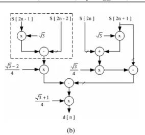
To design data flow of DWT though lifting scheme using Daubechies4 equations, we need to arrange the equations. With appropriate arrangement, the proposed system becomes less complex. Consider equation (7) and (8), which is obtained from solving Daubechies4 equations. There are only 2 equations left to find approximation and detail respectively.
] 3 2 [ ( ]) 1 2 [ 3 ] 2 [ {( 2 1 3 ] [n = − S n + S n+ − S n+ s
3( [2 2] 3 [2 3]) 4 1 + + + − S n S n
( [2 ] 3 [2 1]))} 4 2 3 − + + − S n S n
(7)
] 2 [ ( 3 4 1 ] 1 2 [ { 2 1 3 ] [n S n S n d = + + −( [2 2] 4 2 3 ]) 1 2 [ 3 + − − − + S n S n ])} 1 2 [ 3 − + S n
(8)
After that, these equations are used to make data flow as shown in Fig. 6(a) and (b). From both figures, we can notice that there are some overlapped parts. Therefore, we can combine these parts together to save environment resource as shown in Fig.7.(a)
(b)
Fig. 6 Data flow of low pass filter and high pass filter used to find approximation (a) and detail (b).
Fig. 6 Complete data flow.
3. EXPERIMENT
In our experiment, we selected images form the set of standard ISO test image with resolution of 256 x 256 pixels. Example image used to test DWT transform is show in Fig.8. We begin by loading an image to the memory. Next, image in memory is read by FPGA to process as shown in Fig. 8 (b). Then, we increase image brightness by 128 to the parts of LH, HL, and HH for clarity of details. After that we use result data to be an input and reconstruct image to check the error. The process is tested on real time system. The proposed architecture is implemented as explained in previous sections. From the experiment, we found that our system can process 30 images within an average of 1 second as shown in table 1.
Our experiment system use devices and equipments as followed:
• FPGA Board: FPGA Xilinx Virtex-II 1000 with SDRAM 64MByte.
• PC: CPU Intel Pentium III 1.13 GHz ( Tulatin ), SDRAM 768MByte
ICCAS2005 June 2-5, KINTEX, Gyeonggi-Do, Korea
(a) (b) (c)
Table1Processing time for our system.1 Image Error 30 Images Error PC. 0.089843 Sec. 0 2.644531 Sec. 0 FPGA 0.015236 Sec. 0 0.5470958 Sec. 0
4. CONCLUSION
In this paper, a design of parallel architecture for wavelet transformation on FPGA presented. We begin the design with floating-point computational unit, this unit is essential because it is arranged according to Daubechies4 though lifting. The objective of this paper is to apply FPGA to DWT process to reduce processing time. From the experiment, we found that our system can work on real-time system. System can process 30 images in less than 1 second. However, processing time depends on many factors such as memory speed, CPU speed on the board, because data will be sent and received from CPU all the time. The proposed architecture can be applied on the variety systems such as real time image compression, image quantization, and JPEG 2000. Furthermore, the proposed DWT can perfectly reconstruct data and can be applied in lossless applications.
REFERENCES
[1] CK Chui, “An Introduction to Wavelet,” 1 ed. Wavelet
analysis and its application, Vol. 1. 1992.
[2] S Mallat, “A wavelet tour of signal processing,” 2 ed. 1998.
[3] N Fliege, Multiraten-Signalverarbeitung. Informationstechnik,
ed. N. Fliege. 1993.
[4] J.A. Eldon and C. Robertson, “A Floating Point Format for Signal Processing,” Proceedings IEE International
Conference on Acoustics, Speech, and Signal Processing,
pp. 717-720, 1982.
[5] N. Shirazi, Implementation of a 2-D Fast Fourier
Transform on an FPGA Base Computing Platform,
VPI&SU Masters Thesis in progress. VPI&SU Masters Thesis in progress.
[6] IEEE Task P754, “A Proposed for Binary Floating-Point Arithmetic,” IEEE Computer, Vol. 14, No. 12, pp.51-62, March 1981.
[7] I Daubechies and W Sweldens, Factoring transform into
lifting step, J. Fourier Anal. Appl., pp. 27, 1998.
[8] W Sweldent. “The lifting scheme: Anew philosophy in biorthogonal wavelet constructions,” In Wavelet
Application in Signal and Image Processing III. 1995.
[9] J.M Aronold, D.A Buell and E.G. Davis, “Splash 2,” Proceedings of the 4th Annual ACM Symposium on Parallel Algorithms and Architectures, pp. 316-322, June 1992.
[10] Xilinx, Inc., Programmable Logic Design Quick Start
Handbook, Karen Parnell and Nick Mehta, 2003.