P1-95 / Z. Fanghu
i
IMID 2009 DIGEST •
Abstract
In this paper, chalcogenide glasses material(Se, Te, Sb) is firstly used as encapsulation layer of OLEDs under high vacuum of 10-4Pa. In the experiments, properties of OLEDs
encapsulated by Se, Te, Sb thin film is compared with that of device encapsulated by traditional method. It is found that Se, Te, Sb film can extend lifetime of devices to 1.4, 2, 1.3 times respectively. Chalcogenide glasses film as encapsulation layer has little effect on some characteristics of device. The research indicated that OLEDs can be well protected upon applying Se, Te, Sb film as encapsulation layer. It is clear that it can prolong the lifetime obviously.
1. Introduction
The organic light-emitting materials are severely sensitive to oxygen and moisture [1]. On the one hand, oxygen is a quencher which can make qua ntum efficiency decrease significantly and oxidation the hole transport layer declines its transport ability. On the other hand, organic compounds are hydrolyzed by moisture which makes its stability drop sharply [2-4], and the lifetime of device is shortened finally [5-6]. In order to avoid degradation and invalidation of OLEDs during long-term operation, the high barrier property of packaging material shows very important [7] . Meanwhile, packaging technology is a breakthrough point that can solve lifetime problem of OLEDs [8]. Temporary technique is using desiccant and glass or polymer film which has disadvantages of encapsulation in dry and high purity N2 glove box and complicated technology. In this paper, the influence of chalcogenide glasses(Se、Te、Sb) film encapsulation layers and lifetime of OLEDs was researched and discussed, which were vapored in the high vacuum on protecting of the devices.
2. Experimental
In this paper, Se, Te, Sb were used as encapsulation layer respectively (purity of 99.999%, produced by Xi ’an chemical reagent factory). The devices were prepa red with structure of ITO/CuPc/NPB/Alq3/LiF/Al/ Se,
Te,Sb, as figure 1 shows. OLEDs based on ITO as the anode and LiF/Al as the cathode , phthaloeyanine(CuPc) as the hole injection layer, N, N′- diphenyl-N, N′-bis(1-naphthy1)-(1,1′bipheny1)-4, 4′-diamine(NPB) as the hole transport layer, tris(8-quinolinolato)aluminum complex(Alq3) as the emittin g layer and electrons transport layer and C545T(2%) i s green doped materials. Moreover, Current density-Voltage, Luminance-density-Voltage, Electroluminescence-Voltage. Electroluminescence-spectra and Luminance-Time characteristics, were measured and discussed se parately. ITO substrates with a sheet resistance ranged from 10Ω/□ to 15Ω/□ were etched to form objected p attern and used as anode. After baking, it was sent to i on bombarding chamber for improving smoothness an d work function of the ITO surface. The bombarding c hamber works in the condition of pure oxygen with pr essure of 16Pa. bombarding under discharging voltage of 100V-150V lasts for 10 minutes.
Organic materials and Se,Te,Sb were put in differen t temperature-controlled quartz crucible respectively. Deposition process follows the structure demanded. t he chamber vacuum was kept 7 × 10⁴ Pa, the thicknesses of function layers is CuPc (20n m), NPB(100nm), Alq3 with C545T(2%) doped (80nm)
, Alq3 (70nm), LiF(0.5nm), Al(100nm). It is noteworth
y that the host and dopant were simultaneously deposi ted during the deposition of EL monolayer, achieving designed D/H ratio (dopant/host) by relative evaporate
Effects of Chalcogenide Glasses Thin Film
Encapsulation Layer on Lifetime of Organic
Light Emitting Diodes
Zhang Fanghui, Xi Jianfei and Xi Jianfei
College of Electrical and Information Engineering ,Shaanxi University of
Science & Technology, Xi’an, Shaanxi 710021,China
TEL:86-029-86168956, e-mail:
[email protected]
Keywords : OLEDs; Chalcogenide glasses; film capsulation; lifetimeP1-95 / Z. Fanghu
i
• IMID 2009 DIGEST
Fig.3 Brightness(cd/m2) vs voltage(V)
Fig.2 Current density(J) vs voltage (V).
Figure 1 Structure of OLEDs and materials used.
on speed.Under high vacuum condition, the Se,Te,Sb were deposited on the cathode layers promptly, and then glass cover for encapsulation was applied in the low vacuum.
Evaporation speed is about 0.1-0.3nm/s for organic materials and 0.5nm/s for metal cathode. The evaporation condition of all kinds of thin film encapsulation layers were showed as Tab.1.
TABLE 1. Evaporation condition of encapsulation layer. MATERIALS TEMPERA- TURE (℃) VACUUM (Pa) SPEED (nm/s) Se 90 7×10⁻⁴ 0.1 Te 199 7×10⁻⁴ 0.1 Sb 250 7×10⁻⁴ 0.1
Devices with the active area about 5mm×5mm were tested under the room temperature. Testing facilities which used in this process are as follow: EL spectra and CIE coordinate with OPT2000 , voltage and current characteristics with Keithley2400 and MODEL1830-C and luminance with ST-900.
3. Results and discussion
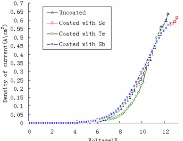
It is well known that OLEDs belong to injecting type light-emitting diodes[9], electrons and holes are injected into emitting layer from cathode and anode respectively, then electrons and holes combine to form excitons under the applied electric field. At last, excitons radiate and emit light. Fig.2 shows Current density-voltage curves of different devices with and without chalcogenide glasses materials Se,Te,Sb. It is found that all devices have low turn-on voltages. The
device encapsulated with Se is about 5V, Te is 5.5V and Sb is 5.2V. and the encapsulation devices have obvious rectifying properties. Furthermore, Se,Te,Sb encapsulation layer almost can’t change turn-on voltage and J-V characteristics of devices.
L-V characteristics of four devices with different encapsulation were shown in Fig.3. Under the positive electrical field, brightness arise with the increase of voltage. Brightness of devices without chalcogenide glasses materials is 25869cd/ m2 when driving
voltage is 11V. Brightness of Se, Te, Sb encapsulated devices is 20000cd/m2, 24399cd/m2, 23800cd/m2,
respectively. Under the same voltage, brightness of uncoated devices is the highest, that of devices using Se, Te, Sb declined slightly. So brightness of devices almost don’t be affected by adding encapsulation layer.
P1-95 / Z. Fanghu
i
IMID 2009 DIGEST • Fig.4 EL spectra of devices.
Fig.5 Brigtness(cd/m2) vs time(H).
EL spectra of four different encapsulation devices a t driving voltage of 8V were showed in Fig.4, devices
coated with Se,Te,Sb have identical peak coordinate and similar FWHM, and all spectral peaks appear at wavelength of 519nm. Encapsulation with Se, Te, Sb gained CIE coordinates as follow: (0.2656, 0.6354), (0 .2684, 0.644), (0.2656, 0.6384). The color of light is g reen. Thus EL spectra also almost can’t be affected by adding chalcogenide materials (Se, Te, Sb).
From Fig.2, Fig.3, Fig.4, it can be found that evapor ation of chalcogenide glasses materials on cathode sur face showed slight effect on main characteristics of O LEDs, Because encapsulation layer is located on catho de layer. Theoretically, it has nothing to do with carrie rs injection, transport as well as recombination.
Brightness decay of four devices is shown in Fig.5. It is found that initial brightness of four devices is 200 0cd/m2, 2200cd/m2, 2000cd/m2, 2000cd/m2 when oper
ational currents is 5.5mA, 5.5mA, 7.0mA, 5.3mA resp ectively. Brightness of device without encapsulation la yer decayed to 1000cd/m2 after 2880 hours. But devic es encapsulated with Se, Te, Sb decayed to 1000cd/m2
after 4000 hours, 5800 hours, 3750 hours respectively. It also can be seen clearly from this figure that bright ness decay becomes slow obviously. Lifetime of OLE Ds is apparently improved by adding Se, Te, Sb encap sulation layer. It is found that Se, Te, Sb film can exte nd lifetime to 1.4, 2, 1.3 times, respectively.
4. Summary
(1) Using chalcogenide glasses as thin film encapsulation layer has little effect on properties of OLEDs.
(2) Lifetime of OLEDs is apparently improved by adding Se, Te, Sb encapsulation layer.
This research was financially supported by the Patent Scientific Research Project of Shaanxi Education Office under Grant NO.07JK191. and the Graduate Innovation Fund of Shaanxi University of Science and Technology.
5. References
[1] Ullrich M, Peter B., The electroluminescence of organic materials[J] Materials Chemistry 10:1471-1507,(2000).
[2] Lim S F,Ke L,Wang W, Chua S J. Correlation between dark spot growth and pinhole size in organic light-emitting diodes[J] Appl Phys Lett 78:2116, (2001).
[3] Nguyen T P, Jolinat P, Destruel P, Clergereaux R, Farenc J. Degradation in organic light-emitting diodes[J] Thin Solid Films 325:175-180 , (1998).
[4] Sheats J R, Roitman D B. Failure modes in polymer-based light-emitting diodes[J].Synthetic Metals 95: 79-85,(1998).
[5] Aziz H, Popovic D Z, Hu NanXing, et al. Degradation mechanism of small molecule-based organic light-emitting devices [ J].Science 283(5409):1 900-1902,(1999).
[6] McElvain J, Antoniadis H, Hueschen M R, et al. Formation and growth of black spots in organic light emitting diodes[J ].Appl.Phys
80(10):6002-P1-95 / Z. Fanghu
i
• IMID 2009 DIGEST
6007,(1996).
[7] Nguyen T P, Jolinat P, Destruel P, et al. Degradation in organic light-emitting diodes [J]. Thin Solid Films 325 (1):175-180, (1998).
[8] Bo Dong, Liying Yang, Danqin Ye et al. Encapsulation technologies of organic light emitting devices[J].Liquid and display 22(2):176-181,(2007).
[9] Woo H S,Czerw R,Webster S.Hole blocking in carbon nanotube-poolymer compo site organic base on ploy [J].Applied Physics Letters, 77(9):1393-1395,(2000).