Direct observation and analysis of yolk-shell materials using low-voltage
high-resolution scanning electron microscopy: Nanometal-particles encapsulated in
metal-oxide, carbon, and polymer
Shunsuke Asahina, Mitsuo Suga, Hideyuki Takahashi, Hu Young Jeong, Carolina Galeano, Ferdi Schüth, and Osamu Terasaki
Citation: APL Materials 2, 113317 (2014); doi: 10.1063/1.4902435 View online: http://dx.doi.org/10.1063/1.4902435
View Table of Contents: http://scitation.aip.org/content/aip/journal/aplmater/2/11?ver=pdfcov Published by the AIP Publishing
Articles you may be interested in
Publisher’s Note: “Direct observation and analysis of yolk-shell materials using low-voltage high-resolution scanning electron microscopy: Nanometal-particles encapsulated in metal-oxide, carbon, and polymer” [APL Mater. 2, 113317 (2014)]
APL Mat. 3, 029901 (2015); 10.1063/1.4906321
Chemoradiotherapeutic wrinkled mesoporous silica nanoparticles for use in cancer therapy APL Mat. 2, 113315 (2014); 10.1063/1.4899118
Macroscopic and microscopic defects and nonlinear optical properties of KH2PO4 crystals with embedded TiO2 nanoparticles
J. Appl. Phys. 112, 014315 (2012); 10.1063/1.4733301
Preparation and characterization of titania nanotubes and hybrid materials derived from them J. Vac. Sci. Technol. B 23, 2398 (2005); 10.1116/1.2122827
Comparison of the agglomeration behavior of thin metallic films on Si O 2 J. Vac. Sci. Technol. A 23, 1152 (2005); 10.1116/1.1861943
and Osamu Terasaki2,4,b
1JEOL Ltd., SM Business Unit, Tokyo, Japan
2Graduate School of EEWS, WCU/BK21+, KAIST, Daejeon 305-701, South Korea 3Department of Heterogeneous Catalysis, Max-Planck-Institut für Kohlenforschung, Mülheim, Germany
4Department of Materials and Environmental Chemistry, Berzelii Centre EXSELENT on Porous Materials, Stockholm University, SE-10691 Stockholm, Sweden
(Received 16 October 2014; accepted 12 November 2014; published online 1 December 2014; corrected 15 December 2014)
Nanometal particles show characteristic features in chemical and physical prop-erties depending on their sizes and shapes. For keeping and further enhancing their features, the particles should be protected from coalescence or degradation. One approach is to encapsulate the nanometal particles inside pores with chem-ically inert or functional materials, such as carbon, polymer, and metal oxides, which contain mesopores to allow permeation of only chemicals not the nanometal particles. Recently developed low-voltage high-resolution scanning electron micros-copy was applied to the study of structural, chemical, and electron state of both nanometal particles and encapsulating materials in yolk-shell materials of Au@C, Ru/Pt@C, Au@TiO2, and Pt@Polymer. Progresses in the following categories were
shown for the yolk-shell materials: (i) resolution of topographic image contrast by secondary electrons, of atomic-number contrast by back-scattered electrons, and of elemental mapping by X-ray energy dispersive spectroscopy; (ii) sample preparation for observing internal structures; and (iii) X-ray spectroscopy such as soft X-ray emission spectroscopy. Transmission electron microscopy was also used for charac-terization of Au@C. C 2014 Author(s). All article content, except where otherwise
noted, is licensed under a Creative Commons Attribution 3.0 Unported License. [http://dx.doi.org/10.1063/1.4902435]
An approach of encapsulation of nano particles with inert or functional shells containing meso-pores has attracted a lot of attentions.1The shell will allow to transfer reactants to and products from
the particles. Nanometal particles (metal= Au, Pt, Pd, and Rh) have been known as important catalysts and their catalytic reactions occur at their surfaces. Size of the nanoparticles gives pronounced effect on physical/chemical properties, therefore it is crucial to have mono-dispersed particles in nano-size regime and to prevent the nanoparticles from coalescence upon heating during reactions. Recently yolk-shell materials, that are the colloidal metal nanoparticles encapsulated in hollow sphere shells as cores, have been developed by Schüth and his group.2They synthesized them through the following processes: colloidal metal nanoparticles with uniform size (as a yolk); covered with silica (as an egg white); coated with thin layer of carbon or metal oxides (TiO2, ZrO2) or polymers (as a shell); and
finally silica is dissolved. In order to enhance catalytic properties of yolk-shell nanoparticles, various
aPresent address: UNIST Central Research Facilities, UNIST, Ulsan 689-798, South Korea.
bAuthor to whom correspondence should be addressed. Electronic addresses:[email protected]and
113317-2 Asahina et al. APL Mater. 2, 113317 (2014)
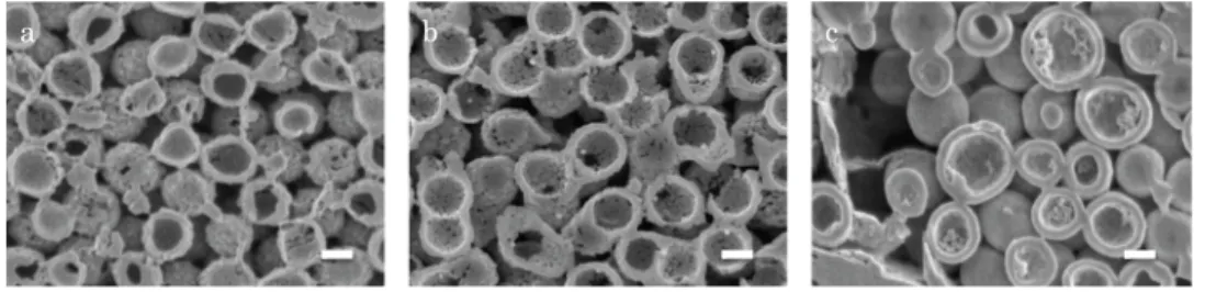
FIG. 1. Low voltage SEM images of Ru/Pt@Carbon (a), Au@Carbon (b), and Pt@Polymer (c). All samples were placed on a holder cooled with liquid nitrogen to reduce damages and cross-sectioned by Ar ion. The images were taken at landing energy of 0.5 keV (a), 2.0 keV (b), and 0.5 keV (c), respectively, while keeping specimen bias voltage at −5 kV. Scale bars: 100 nm.
experimental parameters should be controlled for examples on (i) the cores; elements, alloys, and sizes and shape, (ii) the shells; interacting or non-interacting support for the cores, permeation of various chemicals in and out to the nanoparticles through mesopores existing in the shells but not of nanoparti-cles themselves, hold mechanical strength, and electric conductor or insulator, and (iii) the egg white; create a space between cores and shells to accommodate chemicals and to enhance reactions.
Based on the above points, it is natural to use electron microscopy (EM) for structural and chem-ical characterizations of the yolk-shell materials. Transmission electron microscopy (TEM) gives projected structural information with atomic resolution, while scanning electron microscopy (SEM) gives topographic and surface selective information although spatial resolution is not so high as TEM. Combining both TEM and SEM is ideal. The superiority of the SEM with respect to other microscopes including an optical one is, in particularly, the high spatial resolution with large depth of field, that is, we can observe surface-topological information in high resolution as 3D-panorama even from a large specimen area with large height difference and thick sample. However, in order to utilize full power of SEM, we need to develop suitable methods in sample preparation to observe internal structure of yolk and shell parts at different heights, to reduce electron beam damages, to reduce electron accumulation on surface in electrical insulators, and to observe electron states and elemental map of constituents.3 Here, we start with the development of cross-sectioning and move to some of proper images corresponding to the three points mentioned above. We discuss the current detection limit in terms of elemental and electronic states for the systems we are studying. Then, the advantages of low voltage high resolution SEM (LV-HRSEM) for observing fine structure, elemental, and electronic information of yolk-shell materials are shown and future necessary developments will be discussed.
In order to observe internal structures of nanomaterials by SEM, we need to use a cross-section instrument without inducing so much surface damage to the materials. Key points are to minimize sur-face normal component of momentum of gas ions and not to raise specimen temperature by releasing heat, which is induced by collisions of the ions, quickly from specimen. A device called cross-section polisher (CP) using an argon ion equipped with specimen cooling stage (down to around 120 K at specimen holder during Ar-ion milling) to reduce surface damage was employed.4Low
magnifica-tion SEM images of Ru/Pt@Carbon, Au@TiO2, and Pt@Polymer clearly show advantages of this
approach, uniform sectioning for wide area (Figures1(a)–1(c)), and sectioned surfaces of these mate-rials are less damaged and detailed fine structures by LV-HRSEM images will be shown later.
Recently, a new spectrometer for soft X-ray emission spectroscopy (SXES) has been success-fully developed with energy resolution of 0.3 eV at the Fermi edge of Al-L of Al metal and this can provide highly resolvable soft X-ray emission spectrum at this energy range.5,6Therefore, the SXES will give very valuable information of bonding state while energy dispersive spectroscopy (EDS) can give unresolvable peaks or cannot detect signals in this energy range.
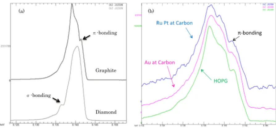
Carbon in Au@Carbon and Ru/Pt@Carbon: C-Kα emission spectrum is strongly influenced with outer molecular orbital, which is composed of several σ-bonding and π-bonding energy bands. As shown in Figure2, C-Kα spectra of carbon in Au@Carbon and Ru/Pt@Carbon are compared with that of HOPG (highly oriented pyrolytic graphite). Several humps are observed in these spectra. The hump at higher energy side is influenced with π-bonding bands as marked in the figure. From this, it is clear that carbon of Ru/Pt@Carbon and Au@Carbon has graphitic feature in electronic state.
FIG. 2. Standard C-K spectra of diamond and graphite (a). C-K spectra of the samples Au@Carbon and Ru/Pt@Carbon, and of HOPG for comparison (b) were acquired by SXES.
FIG. 3. HR-TEM image of Au@Carbon and BFTEM image (a), HRTEM image of the multiply twinned Au-nanoparticle with fcc-structure encapsulated in a hollow sphere shell (b), and HRTEM image of the edge of a carbon shell (c). Condition: BFTEM and HRTEM images were acquired by a JEM-ARM200F at 200 kV.
Figure3shows bright field TEM (BFTEM) and high-resolution TEM (HRTEM) images taken with JEOL ARM 200F operated at 200 kV. The BFTEM image clearly shows the yolk-shell structures in which Au nanoparticles are well encapsulated in hollow carbon shells (Figure3(a)). As seen in Figure3(b), the Au nanoparticle has a spherical shape with multiple twins. It is noted that carbon shells have a graphitic structure as shown in Figure3(c). Figures4(a)and4(b)show BF-scanning transmission electron microscope (STEM) and high angle annular dark field (HAADF) STEM images of Au@TiO2samples. Because the Z-contrast in HAADF-STEM images increases with the atomic
number of elements, the Au nanoparticles encapsulated inTiO2shells could clearly be identified with
the brighter contrast as shown in Figure4(b). Electron diffraction (ED) pattern in Figure4(c)confirms that TiO2is an anatase crystal structure with a lattice parameter of a= 3.79 Å and c = 9.51 Å.
FIG. 4. HR-TEM image of Au@TiO2and BF STEM image (a), HAADF STEM image (b), and ED pattern of Au@TiO2(c).
Condition: BF-STEM and HAADF-STEM images were acquired by a JEM-ARM200F with a Cs corrector at 200 kV (Cs = 0, convergence angle: 22 mrad, spot size: 0.1 nm, semiangles for HAADF detector: 67-170 mrad).
113317-4 Asahina et al. APL Mater. 2, 113317 (2014)
FIG. 5. Three different LV-HRSEM images to show dependence of spatial resolution on specimen bias voltage, keeping constant landing energy of 500 eV. They are taken at specimen bias voltages of 0 (a), −2 kV (b), and −5 kV (c), respectively. Scale bars: 100 nm.
Spatial resolution of SEM is strongly related to a diameter of impact electron beam on a sample. At low acceleration voltage, the limiting factors of the resolution come mainly from both spherical and chromatic aberrations, Cs and Cc. In order to improve the circumstance, combined lens of magnetic and electric ones has been developed by applying specimen bias voltage, Vbias. By this approach,
energy of impact electrons (landing energy) will be reduced from e × abs(Vacc) to e × abs(Vacc− Vbias)
(where Vaccis accelerating voltage and both Vaccand Vbiasare negative). The application of negative
bias generates an electrostatic field between the magnetic objective lens and the sample to act as a focusing and retarding field for the impact electrons, and an accelerating field for electrons emitted from the sample. This coexistence of a magnetic field and a retarding electrostatic field produces a larger convergent force against the incident electrons to the sample, which shortens the focal length and generally results in smaller aberrations than those of independent systems.
This effect is explicitly shown by LV-HRSEM images taken from Au nanoparticles in the present experimental configuration as shown in Figures 5(a)–5(c), with sample bias Vbias of 0.0,
−2.0 kV, and −5.0 kV, respectively, where landing energy was kept constant at 500 eV. In order to observe an image from virgin areas, the images were taken from the same sample but by shifting to the neighboring regions. It is very obvious from a comparison of the images that we can not only see finer surface details by increasing a magnitude of sample bias voltage but also clearer cut of the contrast at the edge of nanoparticles.
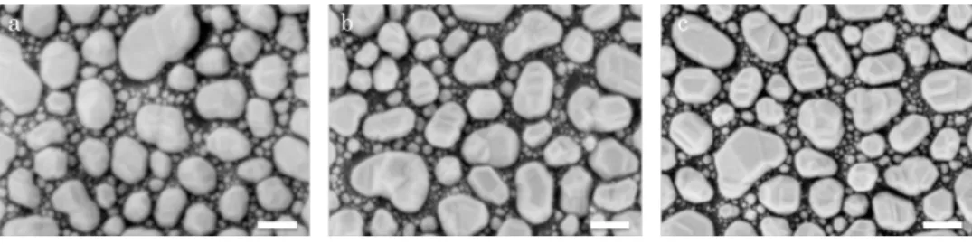
Figure 6 shows surface contrast clearly using LV-HRSEM. The images of Au@Carbon (a), Ru/Pt@Carbon (b), Pt@Polymer (c), and Au@TiO2(d) taken at low landing energy with specimen
bias voltage of −5.0 kV. Those landing energies are selected with optimized condition that means high surface contrast on each material, less electron charge up, or damage. The carbon is one of the difficult materials to visualize topological contrast from the top most surface. However, the surface contrast of carbon goes bright when taken at several hundred eVs. Therefore, the topolog-ical contrast was nicely observed in Figures 6(a)and6(b)at 300 eV and 500 eV, respectively. In addition, Figure6(b)shows compositional contrast from Ru/Pt particles because of higher landing energy, and Figure6(c)is taken at 100 eV to reduce charge up effect and shows nice topological contrast from polymer. For Figure 6(d), 500 eV is used to show topological contrast with high spatial resolution.
Information of surface and internal structure is very important to understand their functions and effects. SEM is one of the techniques that observes surface structures using secondary electron (SE) and back-scattered electron (BSE). To observe internal structures using SEM, cross sectioning of a sample is necessary before SEM operation. However, we need to be careful to prepare cross section on nano structural material for LV-HRSEM observation due to damage from cross sectioning. We used CP. In this system, Ar ions impact the sample parallel to a surface which allows minimization of momentum transfer perpendicular to the surface. Thus, CP is a powerful cross sectional tech-nique for LV-HRSEM. Furthermore, we have recently employed Ar-ion beam cross sectioning with LN2cooling during sample preparation that makes lower ion beam damage during cross sectioning.
The cross-sectioned images of Au@TiO2 and Pt@Polymer are shown in Figure 7. Topological
contrasts with SE are shown in (a) and (c), and compositional contrasts with BSE are shown in (b) and (d). SE images show that particles are exactly inside of hollow sphere. In addition, BSE images show one of the evidence that particles have higher atomic number than hollow spheres.
FIG. 6. LV-HRSEM images of Au@Carbon (a), Ru/Pt@Carbon (b), Pt@Polymer (c), and Au@TiO2(d) taken with specimen
bias voltage −5.0 kV. Landing energies are chosen to give the best images and they are 300, 500, 100, and 500 eV, respectively.
FIG. 7. LV-HRSEM images of Au@TiO2(a) and (b) and Pt@Polymer (c) and (d). SEs are main components in images
(a) and (c), and BSEs are main in images (b) and (d). Experimental conditions for (a), (b), (c), and (d), landing energy and specimen bias, are 2.0 keV, −5.0 kV; 4 keV, 0.0 kV; 0.5 keV, −5.0 kV; and 1.0 keV, 0.0 kV, respectively. Scale bars: 100 nm.
Big progress has been brought into composition analysis using SEM/EDS system: Develop-ment of silicon drifted detector (SDD) significantly enlarged detection area of characteristic X-ray, which enabled big solid angle for X-ray detection. SDD also improved electronic noise and dy-namic range. Owing to these improvements, more characteristic X-rays can be detected, which allowed detection of faint characteristic X-ray signals, signal to noise (S/N) ratio. Thus, a necessary acquisition time of EDS mapping is shortened dramatically. In addition to advantages of SDD,
113317-6 Asahina et al. APL Mater. 2, 113317 (2014)
FIG. 8. EDS analysis on cross-section of Au@TiO2, EDS 150 mm2× 2, landing energy as 4 keV with specimen bias −5 kV,
and probe current at 220 pA.
FIG. 9. SE image of Pt/Ru@Polymer (a) and EDS maps of C (K-line) in red (b), and Ru (L-line) in yellow (c) and Pt (M-line) in green (d), taken at acceleration voltage: 30 kV for 8 min using SDD with 3 units of 150 mm2. Scale bars: 100 nm.
Figure8shows a power of dual EDS system: elemental maps of constituents from cross sectioned Au@TiO2 using dual EDS detectors (detection area of 300 mm2 in total: solid angle of around
0.1 sr). Au nanoparticle with 17 nm in diameter is observed even in 3 min acquisition, and an image accumulated for longer time gives higher quality elemental maps.
Using triple SDD 150 mm2(total detection area of 450 mm2: total solid angle of around 0.2 sr),
we can obtain finer elemental maps as shown in Figure9for Ru/Pt@Polymer. Large detection area increases the solid angle for characteristic X-ray detection and improved sensitivity and S/N in
EXSELENT and 3DEM-NATUR (Sweden, OT), WCU and BK21Plus (Korea, OT) are acknowl-edged.
1F. Schüth,Chem. Mater.26, 423–434 (2014); M. Zhao, K. Deng, L. He, Y. Liu, G. Li, H. Zhao, and Z. Tang,J. Am. Chem. Soc.136, 1738–1741 (2014).
2P. M. Arnal, M. Comotti, and F. Schüth,Angew. Chem., Int. Ed.45, 8224–8227 (2006); P. M. Arnal, F. Schüth, and F. Kleitz, Chem. Commun.1203–1205 (2006); C. Galeano, R. Guettel, M. Paul, P. Arnal, A. H. Lu, and F. Schüth,Chem. - Eur. J.17, 8434–8439 (2011); R. Guettel, M. Paul, C. Galeano, and F. Schüth,J. Catal.289, 100–104 (2012); C. Galeano, C. Baldizzone, H. Bongard, B. Spliethoff, C. Weidenthaler, J. C. Meier, K. J. J. Mayrhofer, and F. Schüth,Adv. Funct. Mater.24, 220–232 (2013); G. H. Wang, J. Hilgert, F. Richter, F. Wang, H. J. Bongard, B. Spliethoff, C. Weidenthaler, and F. Schüth,Nat. Mater.
13, 293–300 (2014).
3O. Terasaki et al., JEOL News 48, 21–31 (2013); M. Suga et al.,Prog. Solid State Chem.42, 1–21 (2014). 4T. Ogiwara, S. Tanuma, Y. Nagasawa, and N. Ikeo, Microbeam Anal. 2, 133–138 (1993).
5M. Terauchi et al.,J. Electron Microsc.61, 1–8 (2012). 6H. Takahashi et al.,Microsc. Microanal.16(S2), 34–35 (2010).