P2-76 / E. Gil
IMID 2009 DIGEST •
Atmospheric pressure plasma deposition of SiO
Xthin films by
direct-Type pin-to-plate dielectric barrier discharge for flexible displays
Elly Gil, June Hee Lee, Yang Su Kim
and Geun Young Yeom
*1
Department of Advanced Materials Science and Engineering, Sungkyunkwan University, Suwon, 440-746, Republic of Korea
Tel. :+82-31-299-6562, E-mail: [email protected]
Keywords: Silicon oxide, PECVD, Atmospheric pressure
Abstract
Silicon dioxide (SiO2) thin films were deposited using a
modified DBD called a “pin-to-plate-type DBD” in order to generate high-density plasmas with a gas mixture of PDMS/O2. The effect of the gas mixture on the
physical and chemical properties of SiO2 deposited by
the pin-to-plate-type DBD with the mixture of PDMS/O2
was investigated.
1. Introduction
SiO2 can be used for passivation and protection of
device surface as the active insulating material. However, in conventional thermal process there can be a deterioration of substrates during deposition of
SiO2 layers, especially in case of polymeric substance.
At low temperature, atmospheric pressure plasma-enhanced chemical vapor deposition (AP-PECVD) techniques present considerable opportunities such as cost-effective depositions and less damaging to the substrates. In particular, the absence of vacuum equipment shows the possibilities of in-line and roll-to-roll processing.
2. Experimental
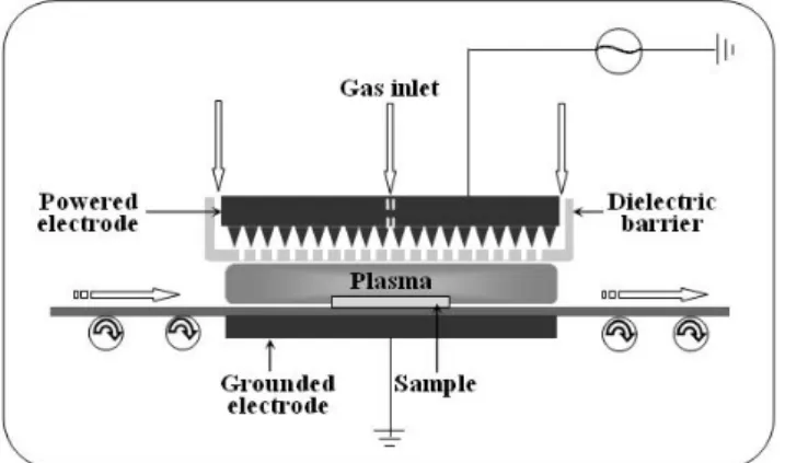
Figure 1 shows the AP-PECVD in-line system used
for the deposition of SiO2. The charge system was
composed of a multi-pin top electrode and a flat-ground electrode separated by about 8 mm. Both electrodes were covered with a 3 mm-thick ceramic plate. Atmospheric pressure plasmas were generated by applying 5 kV AC power (25 kHz) to the multi-pin electrode. Process temperature was maintained below 50℃ using a chiller. The process gas was fed into the system through the shower slit in the ceramic material of the power electrodes.
Fig. 1. Schematic diagram of the AP-PECVD in-line system (pin-to-plate DBD-type).
Polydimethylsiloxane (PDMS) pre-polymer and curing agent (Sylgard 184, Dow Corning) were used as the Si precursors. The chemical structure of PDMS
is composed of repeating –OSi(CH3)2O- units [1]. The
PDMS pre-polymer and curing agent were fed into the system by bubbling He gas through the PDMS liquid reservoir kept at room temperature.
The thickness of the deposited film was measured using a step profilometer (Tencor, Alpha step 500), and the chemical bonding states of the film were measured by X-ray photoelectron spectroscopy (XPS; Thermo Electronics, Multilab ESCA2000) and Fourier transform infrared spectrometry (FT-IR; Bruker IFS-66/S). A Mg source was used as the X-ray source for XPS. The surface of the thin films was observed by field emission scanning electron microscope (FE-SEM; Hitachi, S-4700) and high resolution atomic force microscope (HR – AFM; SII Nano Technology Inc., SPA-300HV).
3. Results and Discussion
P2-76 / E. Gil
• IMID 2009 DIGEST
slm to 15 slm while the O2 gas flow rate was
maintained at 1 slm, the deposition rate was increased almost linearly from 8.1 ± 0.2 nm/min to 23.6 ± 0.4 nm/min. [2] The increased deposition rate was related to the increased silicon source in the gas mixture due to the increased PDMS flow rate, and was, therefore, related to the increased reaction of silicon with oxygen in the gas mixture.
Initially, the deposition rate was increased with O2
flow rate, but then decreased when the O2 gas flow
rate was above 1.0 slm. The increased decomposition of PDMS by oxygen for the formation of silicon oxide [3] brought the initial increase of deposition rate with
the O2 gas flow rate. However, the decrease of
deposition rate with the further increase of O2 gas
flow rate was attributed to the decrease in the dissociation of PDMS due to the increased electron attachment to the oxygen atom which causes the decrease of plasma density [2].
The FT-IR spectra was measured for various PDMS
flow rates (O2 at 1 slm). As the PDMS flow rate was
increased from 7 slm to 15 slm, the peak intensities
related to the Si-OH and the Si-(CH3)x bonding were
also increased. [2]The increase of the Si-OH bonding
peak with increasing PDMS flow rate suggested the presence of a high silanol group ([-OnSi(OH)4-n-]n). In
addition, the increase of the Si-(CH3)x bonding
indicated the possible formation of a soft film rather than hard film due to insufficient oxidation of the dissociated PDMS [2].
Fig. 2. Composition of SiO2 thin films deposited as
a function of the PDMS and O2 flow rate
As shown in Fig. 2, the carbon percentage was increased from 1.4 % to 3.0 % as the PDMS flow rate was increased from 7 to 15 slm due to the increase of
Si-(CH3)x bonding in the film. The carbon content as a
function of the O2 flow rate was minimized at 1.0 slm
of O2, possibly due to the optimized oxidation and
dissociation of PDMS.
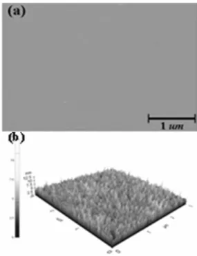
Figure 3 shows the surface micrographs of the thin film deposited at a gas flow rate of PDMS (9 slm
bubbled by He)/O2 1 slm as an optimized process
condition. As shown in fig. 3(a), there were few particles on the surface investigated by SEM. And fig. 3(b) also shows smooth surface by the RMS value of 1.166nm. That was lower value than of reference and the other sample. This is possibly due to particle form-
Fig. 3. The surface morphology of the thin film deposited at PDMS 9 slm, investigated by (a) SEM, (b) AFM.
ation in the gas phase resulting from homogeneous condensation reactions and/or due to porosity in the
thin film resulting from the increased Si-(OH)x
bonding. Also, when the thin film was scratched with tweezers, the film deposited at a higher PDMS flow rate was more easily scratched by the increased Si-(CH3)x bonding, indicating the formation of a soft thin
film which is unsuitable as a water permeation diffusion barrier [4].
4. Summary
pin-P2-76 / E. Gil
IMID 2009 DIGEST •
to-plate, DBD-type, AP-PECVD with a PDMS /O2 gas
at a substrate temperature lower than 50℃ as a
function of the PMDS and O2 gas flow rates.
The increase of PDMS (bubbled through a He flow
at room temperature) at a fixed O2 gas flow rate
increased the deposition rate due to the increased silicon source that was induced by the increased PDMS flow rate. However, the surface roughness was also increased with increasing PDMS flow rate at a
fixed O2 gas flow rate, which was attributed to the
increased porosity in the film due to the increased Si-(OH) bonding in the film, in addition to the possible particle formation in the gas phase by homogeneous
reaction. When the O2 gas flow rate was varied at a
fixed PDMS flow rate, the deposition rate peaked at a
certain O2 flow rate, at which point the surface
roughness was minimized, possibly due to the optimum dissociation and oxidation of PDMS having the lowest Si-(OH) bonding in the film. At an AC power of 5 kV (25 kHz) and at a gas flow rate of
PDMS (9 slm bubbled by He)/O2 1 slm, a SiO2-like,
thin film with a low carbon content of 1.5 % and a smooth surface was obtained at a deposition rate of 12 nm/min.
Acknowledgement
This research was supported by a grant (F0004041-2009-32) from Information Display R&D Center, one of the Knowledge Economy Frontier R&D Program funded by the Ministry of Knowledge Economy of
Korean government.
5. References
1. D. C. Duffy, J. C. McDonald, O. J. A. Schueller, G. M. Whitesides, Anal. Chem., 70, 4974 (1998). 2. J. H. Lee, Y. S. Kim, J. S. Oh, S. J. Kyung, J. T.
Lim, and G. Y. Yeom, J. Electrochem. Soc., 156(7), D248 (2009).
3. J. Pulpytel, F. Arefi-Khonsari, W. Morscheidt, J. Phys. D: Appl. Phys., 38, 1390 (2005).
4. J. H. Lee, Thuy. T. T. Pham, Y. S. Kim, J. T. Lim, S.
J. Kyung, and G. Y. Yeom, J. Electrochem. Soc., 155(3), D163 (2008).