5-1 / B. Cobb
• IMID 2009 DIGEST
Abstract
In this letter we report on the carrier velocity of polycrystalline pentacene transistors as a function of electric field. We performed a series of measurements on devices with a range of channel lengths. At moderate electric fields (<5x10⁵ V/cm), the characteristics are similar to those of disordered or amorphous organic semiconductors. The highest velocities we have measured are near 6 x 104 cm/s at room temperature. We perform quasi-static and dynamic measurements to measure carrier velocity. These results fill an important void between experimental results that have been obtained with disordered/amorphous organic semiconductors and single crystals.
1. Introduction
The carrier velocity versus electric field characteristics of highly disordered organic semiconductors as well as crystalline organic semiconductors have been studied theoretically [1-2] and experimentally [3-5]. In disordered organic semiconductors, the mobility varies with electric field according to the Frenkel-Poole relationship and is given by ln(µ)∝E1/2 where µ is the carrier mobility and E
is the electric field. The velocity is simply the product of the mobility and electric field and varies with electric field as E*exp(γE1/2/kT), where γ and k are constants. In
disordered semiconductors, theoretical models by Bassler and co-workers [1] and the correlated disorder model [2] have been successful at explaining this behavior in materials in which carriers move in a Gaussian density of states with low mobility. In single crystals of organic semiconductors, the velocity can attain values in excess of 106 cm/s at low temperatures.
While the mobility-field characteristics and transport effects within partially disordered polycrystalline organic semiconductors (which are very useful in practical applications such as transistors and solar cells) have been investigated [6-8], there is very little data on velocity-field characteristics. These materials lie in an intermediate region between amorphous organic semiconductors and single crystals. Two reports measure the velocity at specific fields but do not determine the velocity-field characteristic
[9-10]. These characteristics are very useful in designing and analyzing fast circuits as will be discussed below.
2. Experimental
Two methods are employed to measure the velocity-field characteristics. In the first, the field-dependent mobility is measured using transistors with channel lengths in the
range 500 nm to 5 µm on the same substrate.
Measurements are made in the linear region of operation in a field-effect transistor, in which the lateral electric field along the channel is relatively constant. The gate voltage is held at the same value in all measurements, keeping the carrier density approximately the same and eliminating one important cause of change in carrier mobility. The mobility is extracted from well-known current-voltage expressions for the linear region of a field-effect transistor (FET). The lateral electric field is given by VDS/L. where VDS is the drain-source voltage and L is the channel length.
Figure 1 shows the structure of the FETs used in these measurements and the output current-voltage characteristic of one device.
One source of error in measuring mobilities as described above is that we do not account for the voltage drop at the source and drain contacts. The true value of VDS is less
than the apparent value, which leads to an underestimation
of linear mobility. The error in VDS cancels out; thus, the
velocity measurements are not affected by the voltage drops at the contacts, which can be quite substantial. The associated field values, however, are still affected by this source of error, resulting in some overestimation of the lateral electric field.
Dynamic Response and Carrier Velocity in Organic Field-Effect Transistors
Brian Cobb1, Liang Wang1,2, Lawrence Dunn1,and Ananth Dodabalapur1
1Microelectronics Research Center, The University of Texas at Austin, Austin, Texas
78758, U.S.A
E-mail: [email protected]
5-1 / B. Cobb IMID 2009 DIGEST • 0 -5 -10 -15 -20 -25 -30 -35 -40 0 -2ٛ -4ٛ -6ٛ -8ٛ -10ٛ 0V -8V -16V -24V -32V Id (A ) Vds (V) -40V
Fig. 1. ID-VDS output characteristics for a 5 µm channel
length transistor. Inset: Device structure.
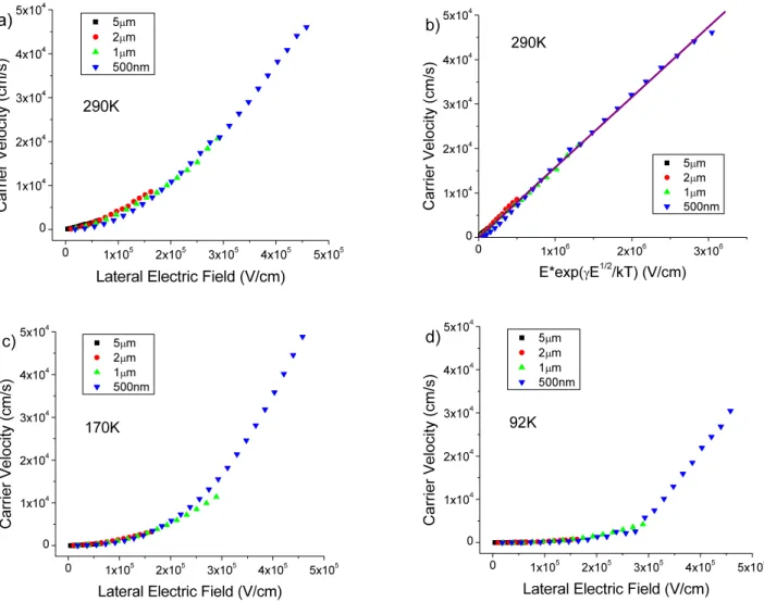
0 1x10⁵ 2x10⁵ 3x10⁵ 4x10⁵ 5x10⁵ 0 1x10⁴ 2x10⁴ 3x10⁴ 4x10⁴ 5x10⁴ 290K Ca rrie r V elo cit y ( cm /s)
Lateral Electric Field (V/cm)
5µm 2µm 1µm 500nm a) 0 1x10⁵ 2x10⁵ 3x10⁵ 4x10⁵ 5x10⁵ 0 1x10⁴ 2x10⁴ 3x10⁴ 4x10⁴ 5x10⁴ c) 170K Ca rrie r V elo cit y ( cm /s)
Lateral Electric Field (V/cm)
5µm 2µm 1µm 500nm
3. Results and discussion
The measured velocity as a function of source drain field is shown in Figure 2 at three temperatures. The gate voltage is held at -40 V in all the measurements keeping the
carrier density approximately the same. Figure 2 is the central result of this letter and indicates that the velocity-field relationship is very similar to that expected for disordered organic semiconductors. In this regime, the mobility-field relationship is Frenkel-Poole like, as previously reported.
Figure 2b displays the carrier velocity plotted against the form E* exp(γE1/2/kT). As expected, from the
Frenkel-Poole model, the data points lie in a straight line. The value of γ = 7 x 10⁻⁵ eV/(V/cm)1/2 was chosen through
fitting the data over multiple temperatures [11]. We
reiterate that the high field data comes from the shorter channel length devices, in which the errors in mobility calculation become larger due to the large voltage drops at the contacts [12-13]. However, the velocity calculation does not suffer from this limitation since the same error (due to the VDS value) that appears in the mobility
calculation is eliminated when the velocity is calculated.
0 1x10⁶ 2x10⁶ 3x10⁶ 0 1x10⁴ 2x10⁴ 3x10⁴ 4x10⁴ 5x10⁴ b) Ca rrie r V elo cit y ( cm /s) E*exp(γE1/2/kT) (V/cm) 5µm 2µm 1µm 500nm 290K 0 1x10⁵ 2x10⁵ 3x10⁵ 4x10⁵ 5x10⁵ 0 1x10⁴ 2x10⁴ 3x10⁴ 4x10⁴ 5x10⁴ d) 92K Ca rrie r V elo cit y ( cm /s)
Lateral Electric Field (V/cm)
5µm
2µm
1µm
500nm
The highest value for the carrier velocity we are able to
measure is ~ 6 x 104 cm/s. Interestingly this value was
obtained at all of the temperatures reported in this work, suggesting that at the high electric fields encountered in measurement conditions, field-assisted hopping is more Fig. 2. Velocity vs. lateral field plots at temperatures of (a) 290 K, (c) 170 K, and (d) 92 K. (b) displays the
5-1 / B. Cobb
• IMID 2009 DIGEST
important than thermal activation. This is a reasonable finding given that at a field of 5 x 10⁵ V/cm, the potential
drop over 0.4 nm (the intermolecular spacing), is about 20 mV, comparable to the value of kT/q at room temperature.
Karl et al. found that at 60 K (the highest temperature reported in their study), the carrier velocity of holes in the c direction in deuterated naphthalene is about 5 x 105 cm/s at
a field of 4 x 10⁴ V/cm [3].
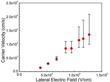
The data described above are all derived from quasi-static measurements. It will be useful to check whether we get similar velocities from dynamic measurements in which the velocity is calculated from a transient response. We have reported how the drift mobility can be measured by applying a step voltage to the source electrode with the gate held at ground and the drain at a potential very close to ground [14-15]. Results from such measurements on pentacene are described in Fig.3, which shows the drift velocity as a function of drain-source voltage (which also equals the gate-source voltage in these measurements) in 7.5 µm channel length devices. At 290 K and a carrier density approximately equal to that employed in the quasi-static measurements (Cox x VGS ≈ 7.5 x 10¹² carriers/cm2),
the velocity is between 5 x 10³ and 1 x 104 cm/s, in very
close agreement with the data of Figure 2. This verification of the velocity measurement by an independent technique based on dynamic measurements is very encouraging. We note that in such dynamic measurements it has so far not been possible to independently vary the carrier concentration and the lateral electric field.
0.0 5.0x10⁴ 1.0x10⁵ 1.5x10⁵ 0.0 5.0x10³ 1.0x10⁴ 1.5x10⁴ 2.0x10⁴ 2.5x10⁴ Ca rrie r V elo cit y ( cm /s)
Lateral Electric Field (V/cm)
Fig. 3. Transient velocity of a pentacene device calculated from the finite response time measured upon application of a voltage step to the source of the device. Error bars represent the finite rise time of the incident voltage step, which creates uncertainty in the true carrier transit time.
Apart from fundamental interest, knowledge of the velocity vs. field characteristics is important in the design and analysis of electronic circuits employing organic transistors. In non-quasistatic circuits such as rectifiers
and frequency dividers that are important in radio-frequency identification tags, knowledge of the velocity-field characteristic is critical to the design process [16]. The dynamic responses of such circuits are transit-time limited and not RC limited. The ultimate performance limits of organic transistor based circuitry can also be estimated from these values.
Studying the behavior of mobility and velocity at varying fields along the transistor channel, insight is gained into the charge transport mechanism in polycrystalline organic semiconductors. At low fields, thermally-assisted hopping over a barrier dominates, which gives rise to the temperature dependence; then at higher fields, field-assisted hopping takes over, and field-dependent mobility is observed while retaining some temperature dependence. This mechanism explains the trend for velocities to approach the same level at higher fields for all the temperatures reported in this work.
4. Summary
We have reported the velocity-field characteristics of pentacene thin-film transistors. The velocities were extracted from the quasi-static measurements of field-dependent mobilities and the electric field. The velocities reach the mid 104 cm/s level at fields of 5 x 10⁵ V/cm.
The nature of the velocity-field curve is similar to that predicted by the Frenkel-Poole relationship. A second measurement method based on dynamic measurements of drift velocity corroborated our quasi-static measurement results.
The authors wish to thank DARPA-MTO, NSF-ECCS, AFOSR, and CONTACT for financial support if this work. They wish to thank Dharmendar Reddy for several helpful discussions.
5. References
1) H. Bässler, Phys. Status Solidi B Vol. 15, 175 (1993). 2) S.V. Novikov, D.H. Dunlap, V.M. Kenkre, P.E. Parris,
A.V. Vannikov, Phys. Rev. Lett. Vol. 81, No. 20, 4472 (1998).
3) W. Warta, N. Karl, Phys. Rev. B Vol. 32, No. 2, 1172-1182 (1985).
4) N. Karl, Synthetic Metals. Vol. 133-134, 649-657 (2003).
5) P. M. Borsenberger, J. Shi, Phys. Status Solidi B Vol. 191, 461 (1995).
6) L. Fumagalli, M. Binda, D. Natali, M. Sampietro, E. Salmoiraghi, P. Di Gianvincenzo, J. Appl. Phys. Vol. 104, 8 (2008).
7) S. F. Nelson, Y. Y. Lin, D. J. Gundlach, T. N. Jackson, Appl. Phys. Lett. Vol. 72, 1854-1856 (1998).
8) J. G. Laquindanum, H. E. Katz, A. J. Lovinger, A. Dodabalapur, Chem. Mat. Vol. 8, 2542 (1996). 9) M. Kitamura, T. Idama, S. Kako, Y. Arakawa, Jpn. J.
5-1 / B. Cobb
IMID 2009 DIGEST •
10) T. Manaka, M. Nakao, E. Lim, M. Iwamoto, Appl. Phys. Lett. Vol. 92, 142103-142106 (2008).
11) L. Wang, D. Fine, D. Basu, A. Dodabalapur, J. Appl. Phys. Vol. 101, 54515 (2007).
12) Y. Chen, I. Shih, J. Mat. Sci. Vol. 44, 280-284 (2009). 13) L. Herlogsson, Y. Y. Noh, N. Zhao, X. Crispin, H.
Sirringhaus, M. Berggren, Adv. Mat. Vol. 20, 4708 (2008).
14) L. Dunn, D. Basu, L. Wang, A. Dodabalapur, Appl. Phys. Lett. Vol. 88, 63507 (2006).
15) L. Dunn, B. Cobb, D. Reddy, A. Dodabalapur, Appl. Phys. A. Vol. 95, 153-158 (2009).
16) R. Rotzoll, S. Mohapatra, V. Olariu, R. Wenz, M. Grigas, K. Dimmler, O. Shchekin, A. Dodabalapur, Appl. Phys. Lett. Vol. 88, 123502 (2006).